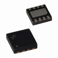
FAN3224CMPX Fairchild Semiconductor, FAN3224CMPX Datasheet - Page 3

FAN3224CMPX
Manufacturer Part Number
FAN3224CMPX
Description
IC GATE DRVR DUAL NONINV 4A 8MLP
Manufacturer
Fairchild Semiconductor
Type
Low Sider
Datasheet
1.FAN3223TMX.pdf
(25 pages)
Specifications of FAN3224CMPX
Configuration
Low-Side
Input Type
Non-Inverting
Delay Time
18ns
Current - Peak
5A
Number Of Configurations
2
Number Of Outputs
2
Voltage - Supply
4.5 V ~ 18 V
Operating Temperature
-40°C ~ 125°C
Mounting Type
Surface Mount
Package / Case
8-MLP
Rise Time
20 ns
Fall Time
17 ns
Supply Voltage (min)
4.5 V
Supply Current
0.95 mA
Maximum Operating Temperature
+ 125 C
Mounting Style
SMD/SMT
Minimum Operating Temperature
- 40 C
Number Of Drivers
2
Lead Free Status / RoHS Status
Lead free / RoHS Compliant
High Side Voltage - Max (bootstrap)
-
Lead Free Status / Rohs Status
Lead free / RoHS Compliant
Other names
FAN3224CMPXTR
Available stocks
Company
Part Number
Manufacturer
Quantity
Price
Company:
Part Number:
FAN3224CMPX
Manufacturer:
XG
Quantity:
11 700
© 2007 Fairchild Semiconductor Corporation
FAN3223 / FAN3224 / FAN3225 • Rev. 1.0.6
Pin Definitions
Output Logic
Note:
7.
Name
OUTA
OUTB
OUTA
OUTB
GND
INA+
INB+
ENA
ENB
VDD
INA-
INB-
INA
INB
P1
Default input signal if no external connection is made.
ENx
1
1
0
0
FAN3223 (x=A or B)
(7)
(7)
Enable Input for Channel A. Pull pin LOW to inhibit driver A. ENA has TTL thresholds for both TTL and
CMOS INx threshold.
Enable Input for Channel B. Pull pin LOW to inhibit driver B. ENB has TTL thresholds for both TTL and
CMOS INx threshold.
Ground. Common ground reference for input and output circuits.
Input to Channel A.
Non-Inverting Input to Channel A. Connect to VDD to enable output.
Inverting Input to Channel A. Connect to GND to enable output.
Input to Channel B.
Non-Inverting Input to Channel B. Connect to VDD to enable output.
Inverting Input to Channel B. Connect to GND to enable output.
Gate Drive Output A: Held LOW unless required input(s) are present and V
Gate Drive Output B: Held LOW unless required input(s) are present and V
Gate Drive Output A (inverted from the input): Held LOW unless required input is present and V
above UVLO threshold.
Gate Drive Output B (inverted from the input): Held LOW unless required input is present and V
above UVLO threshold.
Thermal Pad (MLP only). Exposed metal on the bottom of the package; may be left floating or connected
to GND; NOT suitable for carrying current.
Supply Voltage. Provides power to the IC.
FAN3223
INx
1
1
0
0
(7)
(7)
OUTx
0
0
1
0
Figure 4. Pin Assignments (Repeated)
ENx
1
1
0
0
FAN3224 (x=A or B)
(7)
(7)
Pin Description
FAN3224
3
INx
0
0
1
1
(7)
(7)
OUTx
0
0
0
1
INx+
DD
DD
0
0
1
1
FAN3225 (x=A or B)
(7)
(7)
is above UVLO threshold.
is above UVLO threshold.
FAN3225
INx−
1
1
0
0
(7)
(7)
www.fairchildsemi.com
DD
DD
OUTx
is
is
0
0
1
0


