ISL6596CRZ Intersil, ISL6596CRZ Datasheet - Page 6
ISL6596CRZ
Manufacturer Part Number
ISL6596CRZ
Description
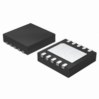
IC MOSFET DRVR SYNC BUCK 10-DFN
Manufacturer
Intersil
Datasheet
1.ISL6596CRZ.pdf
(11 pages)
Specifications of ISL6596CRZ
Configuration
High and Low Side, Synchronous
Input Type
PWM
Delay Time
19ns
Current - Peak
2A
Number Of Configurations
1
Number Of Outputs
2
High Side Voltage - Max (bootstrap)
36V
Voltage - Supply
4.5 V ~ 5.5 V
Operating Temperature
0°C ~ 70°C
Mounting Type
Surface Mount
Package / Case
10-DFN
Lead Free Status / RoHS Status
Lead free / RoHS Compliant
Available stocks
Company
Part Number
Manufacturer
Quantity
Price
Company:

Part Number:
ISL6596CRZ
Manufacturer:
Intersil
Quantity:
900
Part Number:
ISL6596CRZ-T
Manufacturer:
INTERSIL
Quantity:
20 000


Functional Pin Description
Note: Pin numbers refer to the SOIC package. Check
diagram for corresponding DFN pinout.
UGATE (Pin 1)
Upper gate drive output. Connect to gate of high-side
N-Channel power MOSFET. A gate resistor is never
recommended on this pin, as it interferes with the operation
shoot-through protection circuitry.
BOOT (Pin 2)
Floating bootstrap supply pin for the upper gate drive.
Connect a bootstrap capacitor between this pin and the
PHASE pin. The bootstrap capacitor provides the charge
used to turn on the upper MOSFET. See “Bootstrap
Considerations” on page 7 for guidance in choosing the
appropriate capacitor value.
PWM (Pin 3)
The PWM signal is the control input for the driver. The PWM
signal can enter three distinct states during operation, see
“PWM Input and Threshold Control” on page 7 for further
details. Connect this pin to the PWM output of the controller.
GND (Pin 4)
Ground pin. All signals are referenced to this node.
Timing Diagram
PWM
UGATE
LGATE
t
PDLL
t
PDHU
1V
t
RU
6
t
PDLU
50% of VCC
t
FIGURE 1. TIMING DIAGRAM
PDHL
1V
t
RL
ISL6596
t
FL
LGATE (Pin 5)
Lower gate drive output. Connect to gate of the low side
N-Channel power MOSFET. A gate resistor is never
recommended on this pin, as it interferes with the operation
shoot-through protection circuitry.
VCC (Pin 6)
Connect this pin to a +5V bias supply. Locally bypass with a
high quality ceramic capacitor to ground.
VCTRL (Pin 7)
This pin sets the PWM logic threshold. Connect this pin to
3.3V source for 3.3V PWM input and pull it to 5V source for
5V PWM input.
PHASE (Pin 8)
Connect this pin to the source of the upper MOSFET. This
pin provides the return path for the upper gate driver current.
Thermal Pad (in DFN only)
The metal pad underneath the center of the IC is a thermal
substrate. The PCB “thermal land” design for this exposed
die pad should include vias that drop down and connect to
one or more buried copper plane(s). This combination of
vias for vertical heat escape and buried planes for heat
spreading allows the DFN to achieve its full thermal
potential. This pad should be either grounded or floating,
and it should not be connected to other nodes. Refer to
TB389 for design guidelines.
t
TSSHD
t
PTS
t
RU
t
TSSHD
t
FU
t
PTS
January 22, 2010
FN9240.1
Related parts for ISL6596CRZ
Image
Part Number
Description
Manufacturer
Datasheet
Request
R

Part Number:
Description:
Synchronous Rectified MOSFET Driver
Manufacturer:
Intersil Corporation
Datasheet:
Part Number:
Description:
Intersil Corporation [CMOS Serial Controller Interface]
Manufacturer:
Intersil Corporation
Datasheet:
Part Number:
Description:
Manufacturer:
Intersil Corporation
Datasheet:
Part Number:
Description:
357-036-542-201 CARDEDGE 36POS DL .156 BLK LOPRO
Manufacturer:
Intersil Corporation
Datasheet:
Part Number:
Description:
1024-Word x 4-Bit LSI Static RAM
Manufacturer:
Intersil Corporation
Datasheet:
Part Number:
Description:
General Purpose NPN Transistor Arrays FN341.4
Manufacturer:
Intersil Corporation
Datasheet:
Part Number:
Description:
CMOS 16-Bit Microprocessor
Manufacturer:
Intersil Corporation
Datasheet:
Part Number:
Description:
Manufacturer:
Intersil Corporation
Datasheet:
Part Number:
Description:
Manufacturer:
Intersil Corporation
Datasheet:
Part Number:
Description:
Manufacturer:
Intersil Corporation
Datasheet:
Part Number:
Description:
Manufacturer:
Intersil Corporation
Datasheet:
Part Number:
Description:
CMOS 6-Bit Latch and Decoder Memory Interfaces
Manufacturer:
Intersil Corporation
Datasheet:
Part Number:
Description:
CA3046General Purpose NPN Transistor Arrays
Manufacturer:
Intersil Corporation
Datasheet:
Part Number:
Description:
Manufacturer:
Intersil Corporation
Datasheet:
Part Number:
Description:
TR909 DLC/FLC SLIC with Low Power Standby
Manufacturer:
Intersil Corporation
Datasheet: