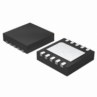
ISL6596CRZ Intersil, ISL6596CRZ Datasheet - Page 9

ISL6596CRZ
Manufacturer Part Number
ISL6596CRZ
Description
IC MOSFET DRVR SYNC BUCK 10-DFN
Manufacturer
Intersil
Datasheet
1.ISL6596CRZ.pdf
(11 pages)
Specifications of ISL6596CRZ
Configuration
High and Low Side, Synchronous
Input Type
PWM
Delay Time
19ns
Current - Peak
2A
Number Of Configurations
1
Number Of Outputs
2
High Side Voltage - Max (bootstrap)
36V
Voltage - Supply
4.5 V ~ 5.5 V
Operating Temperature
0°C ~ 70°C
Mounting Type
Surface Mount
Package / Case
10-DFN
Lead Free Status / RoHS Status
Lead free / RoHS Compliant
Available stocks
Company
Part Number
Manufacturer
Quantity
Price
Company:
Part Number:
ISL6596CRZ
Manufacturer:
Intersil
Quantity:
900
Part Number:
ISL6596CRZ-T
Manufacturer:
INTERSIL
Quantity:
20 000
Application Information
MOSFET Selection
The parasitic inductances of the PCB and of the power
devices’ packaging (both upper and lower MOSFETs) can
cause serious ringing, exceeding absolute maximum rating
of the devices. The negative ringing at the edges of the
PHASE node could increase the bootstrap capacitor voltage
through the internal bootstrap diode, and in some cases, it
may overstress the upper MOSFET driver. Careful layout,
proper selection of MOSFETs and packaging can go a long
way toward minimizing such unwanted stress.
The D
parasitic lead inductances and are not recommended unless
additional circuits are implemented to prevent the BOOT and
PHASE pins from exceeding the device rating. Low-profile
MOSFETs, such as Direct FETs and multi-SOURCE leads
devices (SO-8, LFPAK, PowerPAK), have low parasitic lead
inductances and are preferred.
Layout Considerations
A good layout helps reduce the ringing on the switching
node (PHASE) and significantly lowers the stress applied to
the output drives. The following advice is meant to lead to an
optimized layout:
• Keep decoupling loops (VCC-GND and BOOT-PHASE) as
• Minimize trace inductance, especially on low-impedance
• Minimize the inductance of the PHASE node. Ideally, the
• Minimize the current loop of the output and input power
In addition, for heat spreading, place copper underneath the
IC whether it has an exposed pad or not. The copper area
can be extended beyond the bottom area of the IC and/or
connected to buried power ground plane(s) with thermal
vias. This combination of vias for vertical heat escape,
extended copper plane, and buried planes improve heat
dissipation and allow the part to achieve its full thermal
potential.
short as possible.
lines. All power traces (UGATE, PHASE, LGATE, GND,
VCC) should be short and wide, as much as possible.
source of the upper and the drain of the lower MOSFET
should be as close as thermally allowable.
trains. Short the source connection of the lower MOSFET
to ground as close to the transistor pin as feasible. Input
capacitors (especially ceramic decoupling) should be
placed as close to the drain of upper and source of lower
MOSFETs as possible.
2
-PAK, or D-PAK packaged MOSFETs, have large
9
ISL6596
Upper MOSFET Self Turn-On Effects At Startup
Should the driver have insufficient bias voltage applied, its
outputs are floating. If the input bus is energized at a high
dV/dt rate while the driver outputs are floating, because of
self-coupling via the internal C
UGATE could momentarily rise up to a level greater than the
threshold voltage of the MOSFET. This could potentially turn
on the upper switch and result in damaging inrush energy.
Therefore, if such a situation (when input bus powered up
before the bias of the controller and driver is ready) could
conceivably be encountered, it is a common practice to
place a resistor (R
upper MOSFET to suppress the Miller coupling effect. The
value of the resistor depends mainly on the input voltage’s
rate of rise, the C
threshold of the upper MOSFET. A higher dV/dt, a lower
C
FET will require a smaller resistor to diminish the effect of
the internal capacitive coupling. For most applications, a
5kΩ to 10kΩ resistor is typically sufficient, not affecting
normal performance and efficiency.
The coupling effect can be roughly estimated with the
following equations, which assume a fixed linear input ramp
and neglect the clamping effect of the body diode of the
upper drive and the bootstrap capacitor. Other parasitic
components such as lead inductances and PCB
capacitances are also not taken into account. These
equations are provided for guidance purpose only.
Therefore, the actual coupling effect should be examined
using a very high impedance (10MΩ or greater) probe to
ensure a safe design margin.
V
DS
R
GS_MILLER
FIGURE 5. GATE TO SOURCE RESISTOR TO REDUCE
=
VCC
/C
R
GS
UGPH
ratio, and a lower gate-source threshold upper
UPPER MOSFET MILLER COUPLING
=
+
DU
DL
R
dV
------- R C
dt
GI
GD
UGPH
⋅
/C
⋅
GS
C
PHASE
BOOT
) across the gate and source of the
UGATE
rss
rss
ratio, as well as the gate-source
C
⎛
⎜
⎜
⎜
⎜
⎝
BOOT
1 e
=
–
GD
C
--------------------------------- -
dV
------ - R C
GD
dt
G
of the MOSFET, the
–
⋅
V
DS
R
⋅
C
GI
GD
iss
C
C
⎞
⎟
⎟
⎟
⎟
⎠
iss
GS
S
=
VIN
January 22, 2010
C
Q
GD
UPPER
D
(EQ. 5)
+
FN9240.1
C
C
DS
GS


