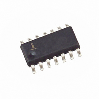
HIP6602BCBZ Intersil, HIP6602BCBZ Datasheet - Page 6

HIP6602BCBZ
Manufacturer Part Number
HIP6602BCBZ
Description
IC DRIVER MOSFET QUAD 14-SOIC
Manufacturer
Intersil
Datasheet
1.HIP6602BCBZ.pdf
(12 pages)
Specifications of HIP6602BCBZ
Configuration
High and Low Side, Synchronous
Input Type
PWM
Current - Peak
400mA
Number Of Configurations
2
Number Of Outputs
4
High Side Voltage - Max (bootstrap)
15V
Voltage - Supply
10.8 V ~ 13.2 V
Operating Temperature
0°C ~ 85°C
Mounting Type
Surface Mount
Package / Case
14-SOIC (3.9mm Width), 14-SOL
Lead Free Status / RoHS Status
Lead free / RoHS Compliant
Delay Time
-
Available stocks
Company
Part Number
Manufacturer
Quantity
Price
Company:
Part Number:
HIP6602BCBZ-T
Manufacturer:
SMD
Quantity:
38
Part Number:
HIP6602BCBZ-T
Manufacturer:
INTERSIL
Quantity:
20 000
Functional Pin Descriptions
PWM1 (Pin 1) and PWM2 (Pin 2), (Pins 15 and 16
QFN)
The PWM signal is the control input for the driver. The PWM
signal can enter three distinct states during operation, see the
three-state PWM Input section under DESCRIPTION for further
details. Connect this pin to the PWM output of the controller.
GND (Pin 3), (Pin 1 QFN)
Bias and reference ground. All signals are referenced to
this node.
LGATE1 (Pin 4) and LGATE2 (Pin 7), (Pins 2 and
6 QFN)
Lower gate drive outputs. Connect to gates of the low-side
power N-Channel MOSFETs.
PVCC (Pin 5), (Pin 3 QFN)
This pin supplies the upper and lower gate drivers bias.
Connect this pin from +12V down to +5V.
PGND (Pin 6), (Pin 4 QFN)
This pin is the power ground return for the lower gate
drivers.
PHASE2 (Pin 8) and PHASE1 (Pin 13), (Pins 7 and
13 QFN)
Connect these pins to the source of the upper MOSFETs
and the drain of the lower MOSFETs. The PHASE voltage is
monitored for adaptive shoot-through protection. These pins
also provide a return path for the upper gate drive.
UGATE2 (Pin 9) and UGATE1 (Pin 12), (Pins 9 and
12 QFN)
Upper gate drive outputs. Connect to gate of high-side
power N-Channel MOSFETs.
Timing Diagram
TPDL
UGATE
LGATE
PWM
LGATE
.
TPDH
UGATE
6
TF
LGATE
TR
UGATE
HIP6602B
TPDL
BOOT 2 (Pin 10) and BOOT 1 (Pin 11), (Pins 10 and
11 QFN)
Floating bootstrap supply pins for the upper gate drivers.
Connect a bootstrap capacitor between these pins and the
corresponding PHASE pin. The bootstrap capacitor provides
the charge to turn on the upper MOSFETs. A resistor in
series with boot capacitor is required in certain applications
to reduce ringing on the BOOT pin. See the Internal
Bootstrap Device section under DESCRIPTION for guidance
in choosing the appropriate resistor and capacitor value.
VCC (Pin 14), (Pin 14 QFN)
Connect this pin to a +12V bias supply. Place a high quality
bypass capacitor from this pin to GND. To prevent forward
biasing an internal diode, this pin should be more positive
then PVCC during converter start-up
Description
Operation
Designed for versatility and speed, the HIP6602B two channel,
dual MOSFET driver controls both high-side and low-side
N-Channel FETs from two externally provided PWM signals.
The upper and lower gates are held low until the driver is
initialized. Once the VCC voltage surpasses the VCC Rising
Threshold (See Electrical Specifications), the PWM signal
takes control of gate transitions. A rising edge on PWM
initiates the turn-off of the lower MOSFET (see Timing
Diagram). After a short propagation delay [TPDL
lower gate begins to fall. Typical fall times [TF
provided in the Electrical Specifications section. Adaptive
shoot-through circuitry monitors the LGATE voltage and
determines the upper gate delay time [TPDH
on how quickly the LGATE voltage drops below 2.2V. This
prevents both the lower and upper MOSFETs from
conducting simultaneously or shoot-through. Once this delay
period is complete the upper gate drive begins to rise
[TR
UGATE
UGATE
] and the upper MOSFET turns on.
TPDH
LGATE
TF
UGATE
TR
LGATE
UGATE
LGATE
LGATE
July 22, 2005
] based
] are
FN9076.5
], the


