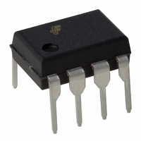
FAN7529N Fairchild Semiconductor, FAN7529N Datasheet - Page 12

FAN7529N
Manufacturer Part Number
FAN7529N
Description
IC PFC CTRLR CRM/TRANSITION 8DIP
Manufacturer
Fairchild Semiconductor
Datasheet
1.FAN7529MX.pdf
(20 pages)
Specifications of FAN7529N
Mode
Critical Conduction (CRM), Discontinuous (Transition)
Current - Startup
40µA
Voltage - Supply
12 V ~ 22 V
Operating Temperature
-40°C ~ 125°C
Mounting Type
Through Hole
Package / Case
8-DIP (0.300", 7.62mm)
Maximum Operating Temperature
+ 125 C
Mounting Style
Through Hole
Minimum Operating Temperature
- 40 C
Lead Free Status / RoHS Status
Lead free / RoHS Compliant
Frequency - Switching
-
Lead Free Status / Rohs Status
Lead free / RoHS Compliant
FAN7529 Rev. 1.0.2
© 2006 Fairchild Semiconductor Corporation
Applications Information
1. Error Amplifier Block
The error amplifier block consists of a transconductance
amplifier, output OVP comparator, and disable compara-
tor. For the output voltage control, a transconductance
amplifier is used instead of the conventional voltage
amplifier. The transconductance amplifier (voltage con-
trolled current source) aids the implementation of OVP
and disable function. The output current of the amplifier
changes according to the voltage difference of the invert-
ing and non-inverting input of the amplifier. The output
voltage of the amplifier is compared with the internal
ramp signal to generate the switch turn-off signal. The
OVP comparator shuts down the output drive block when
the voltage of the INV pin is higher than 2.675V and
there is 0.175V hysteresis. The disable comparator dis-
ables the operation of the FAN7529 when the voltage of
the inverting input is lower than 0.45V and there is
100mV hysteresis. An external small signal MOSFET
can be used to disable the IC, as shown in Figure 33.
The IC operating current decreases below 65µA to
reduce power consumption if the IC is disabled.
2. Zero Current Detection Block
The zero current detector (ZCD) generates the turn-on
signal of the MOSFET when the boost inductor current
reaches zero using an auxiliary winding coupled with the
inductor. If the voltage of the ZCD pin goes higher than
1.5V, the ZCD comparator waits until the voltage goes
Error Amp
Disable
OVP
2
COMP
Figure 33. Error Amplifier Block
Gm
0.45V
2.675V
V
ref1
(2.5V)
0.35V
2.5V
1
INV
V
out
FAN7529 Rev. 00
Disable
Signal
12
below 1.4V. If the voltage goes below 1.4V, the zero cur-
rent detector turns on the MOSFET. The ZCD pin is pro-
tected internally by two clamps, 6.7V-high clamp and
0.65V-low clamp. The 150µs timer generates a MOSFET
turn-on signal if the drive output has been low for more
than 150µs from the falling edge of the drive output.
3. Sawtooth Generator Block
The output of the error amplifier and the output of the
sawtooth generator are compared to determine the
MOSFET turn-off instance. The slope of the sawtooth is
determined by an external resistor connected to the
MOT pin. The voltage of the MOT pin is 2.9V and the
slope is proportional to the current flowing out of the
MOT pin. The internal ramp signal has a 1V offset; there-
fore, the drive output is shut down if the voltage of the
COMP pin is lower than 1V. The MOSFET on-time is
maximum when the COMP pin voltage is 5V. According
to the slope of the internal ramp, the maximum on-time
can be programmed. The necessary maximum on-time
depends on the boost inductor, lowest AC line voltage,
and maximum output power. The resistor value should
be designed properly.
MOT
V
in
Figure 34. Zero Current Detector Block
3
Figure 35. Sawtooth Generator Block
2.9V
R
ZCD
ZCD
5
6.7V
Saw Tooth
Generator
1.4V
1.5V
Error Amp
Output
1V Offset
Zero Current
Detector
150μs
S
R
Timer
www.fairchildsemi.com
FAN7529 Rev. 00
Off Signal
FAN7529 Rev. 00
Q
Turn-on
Signal


