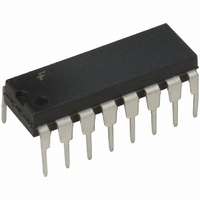
ML4841CP Fairchild Semiconductor, ML4841CP Datasheet - Page 10

ML4841CP
Manufacturer Part Number
ML4841CP
Description
IC CTRLR PFC/PWM VARIABLE 16DIP
Manufacturer
Fairchild Semiconductor
Datasheet
1.ML4841CP.pdf
(15 pages)
Specifications of ML4841CP
Mode
Average Current
Frequency - Switching
200kHz
Voltage - Supply
0 V ~ 7 V
Operating Temperature
0°C ~ 70°C
Mounting Type
Through Hole
Package / Case
16-DIP (0.300", 7.62mm)
Switching Frequency
200 KHz
Maximum Operating Temperature
+ 150 C
Mounting Style
Through Hole
Minimum Operating Temperature
- 65 C
Lead Free Status / RoHS Status
Lead free / RoHS Compliant
Current - Startup
-
Lead Free Status / Rohs Status
Lead free / RoHS Compliant
Other names
ML4841CP_NL
ML4841CP_NL
ML4841CP_NL
Available stocks
Company
Part Number
Manufacturer
Quantity
Price
Company:
Part Number:
ML4841CP
Manufacturer:
ML
Quantity:
5 680
Part Number:
ML4841CP
Manufacturer:
FAIRCHILD/仙童
Quantity:
20 000
ML4841
PWM SECTION
Pulse Width Modulator
The PWM section of the ML4841 is straightforward, but
there are several points which should be noted. Foremost
among these is its inherent synchronization to the PFC
section of the device, to which it also provides its basic
timing. The PWM operates in current-mode. In applications
utilizing current mode control, the PWM ramp (RAMP 2) is
usually derived directly from a current sensing resistor or
current transformer in the primary of the output stage, and is
thereby representative of the current flowing in the con-
verter’s output stage. The DC I
cycle-by-cycle current limiting and is connected to RAMP 2
internally. If the current sense signal exceeds the 1V thresh-
old, the PWM switch is disabled until the protection flip-flop
is rest by the clock pulse at the start of the next PWM power
cycle.
PWM Current Limit
The DC I
iter for the PWM section. Should the input voltage at this pin
ever exceed 1V, the output of the PWM will be disabled until
the output flip-flop is reset by the clock pulse at the start of
the next PWM power cycle.
V
The V
and inhibits the PWM if this voltage on V
nominal 2.5V. Once this voltage reaches 2.5V, which
corresponds to the PFC output capacitor being charged to its
rated boost voltage, the soft-start commences.
PWM Control (RAMP 2)
The PWM section utilizes current mode control. RAMP 2
is generally used as the sampling point for a voltage
representing the current in the primary of the PWM’s output
transformer, derived either by a current sensing resistor or a
current transformer.
Soft Start
Start-up of the PWM is controlled by the selection of the
external capacitor at SS. A current source of 50µA supplies
the charging current for the capacitor, and start-up of the
PWM begins at 1.25V. Start-up delay can be programmed by
the following equation:
where C
is the desired start-up delay.
It is important that the time constant of the PWM soft-start
allows the PFC time to generate sufficient output power for
the PWM section. The PWM start-up delay should be at least
5ms.
10
IN
C
OK Comparator
SS
IN
=
SS
OK comparator monitors the DC output of the PFC
LIMIT
t
DELAY
is the required soft start capacitance, and t
comparator is a cycle-by-cycle current lim-
×
--------------- -
1.25V
50µA
LIMIT
comparator provides
FB
is less than its
DELAY
(11)
Solving for the minimum value of C
Generating V
The ML4841 is a current-fed part. It has an internal shunt
voltage regulator, which is designed to regulate the voltage
internal to the part at 13.5V. This allows a low power dissi-
pation while at the same time delivering 10V of gate drive at
the PWM OUT and PFC OUT outputs. It is important to
limit the current through the part to avoid overheating or
destroying it. This can be easily done with a single resistor in
series with the Vcc pin, returned to a bias supply of typically
18V to 20V. The resistor’s value must be chosen to meet the
operating current requirement of the ML4841 itself (19mA
max) plus the current required by the two gate driver outputs.
EXAMPLE:
With a V
driving a total gate charge of 100nC at 100kHz (1 IRF840
MOSFET and 2 IRF830 MOSFETs), the gate driver current
required is:
To check the maximum dissipation in the ML4841, check the
current at the minimum V
The maximum allowable I
able design.
I
R
I
GATEDRIVE
CC
BIAS
C
Figure 3. External Component Connections to V
SS
=
20V 12.4V
-------------------------------- -
=
=
BIAS
-------------------------------------- -
19mA
5ms
160Ω
20V 14.6V
=
–
(
CC
100kHz 45nC
of 20V, a V
ML4841
×
V BIAS
–
V CC
GND
+
--------------- -
1.25V
50µA
15mA
=
×
47.5mA
=
=
CC
CC
CC
200nF
160Ω
)
ceramic
(12.4V):
limit of 14.6V (max) and
is 55mA, so this is an accept-
10nF
+
(
200kHz 52nC
PRODUCT SPECIFICATION
SS
:
×
ceramic
REV. 1.0.3 6/13/01
1µF
)
=
15mA
CC
(14)
(12)
(13)


