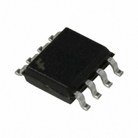
FAN4803CS2 Fairchild Semiconductor, FAN4803CS2 Datasheet - Page 6

FAN4803CS2
Manufacturer Part Number
FAN4803CS2
Description
IC CTRLR PFC/PWM 67/134KHZ 8SOIC
Manufacturer
Fairchild Semiconductor
Datasheet
1.FAN4803CP2.pdf
(12 pages)
Specifications of FAN4803CS2
Mode
Average Current
Frequency - Switching
67kHz
Current - Startup
200µA
Voltage - Supply
10 V ~ 15 V
Operating Temperature
0°C ~ 70°C
Mounting Type
Surface Mount
Package / Case
8-SOIC (3.9mm Width)
Switching Frequency
134 KHz
Maximum Operating Temperature
+ 70 C
Mounting Style
SMD/SMT
Minimum Operating Temperature
0 C
Lead Free Status / RoHS Status
Lead free / RoHS Compliant
Other names
FAN4803CS2_NL
FAN4803CS2_NL
FAN4803CS2_NL
Available stocks
Company
Part Number
Manufacturer
Quantity
Price
Part Number:
FAN4803CS2
Manufacturer:
F
Quantity:
20 000
Company:
Part Number:
FAN4803CS2X
Manufacturer:
FSC
Quantity:
1 000
FAN4803
In the case of leading edge modulation, the switch is turned
OFF right at the leading edge of the system clock. When the
modulating ramp reaches the level of the error amplifier
output voltage, the switch will be turned ON. The effective
duty-cycle of the leading edge modulation is determined
during the OFF time of the switch. Figure 3 shows a leading
edge control scheme.
One of the advantages of this control technique is that it
requires only one system clock. Switch 1 (SW1) turns OFF
and Switch 2 (SW2) turns ON at the same instant to mini-
mize the momentary “no-load” period, thus lowering ripple
voltage generated by the switching action. With such
synchronized switching, the ripple voltage of the first stage
is reduced. Calculation and evaluation have shown that the
120Hz component of the PFC’s output ripple voltage can be
reduced by as much as 30% using this method, substantially
reducing dissipation in the high-voltage PFC capacitor.
Typical Applications
One Pin Error Amp
The FAN4803 utilizes a one pin voltage error amplifier in the
PFC section (VEAO). The error amplifier is in reality a cur-
rent sink which forces 35µA through the output program-
ming resistor. The nominal voltage at the VEAO pin is 5V.
The VEAO voltage range is 4 to 6V. For a 11.3M resistor
chain to the boost output voltage and 5V steady state at the
VEAO, the boost output voltage would be 400V.
6
REF
+
DC
VIN
OSC
I1
L1
U4
+
–
EA
RAMP
CLK
U3
Figure 3. Typical Leading Edge Control Scheme.
VEAO
SW2
SW1
+
–
CMP
U1
I2
C1
I4
I3
R
D
DFF
CLK
U2
RL
Q
Q
Programming Resistor Value
Equation 1 calculates the required programming resistor
value.
PFC Voltage Loop Compensation
The voltage-loop bandwidth must be set to less than 120Hz
to limit the amount of line current harmonic distortion.
A typical crossover frequency is 30Hz. Equation 1, for
simplicity, assumes that the pole capacitor dominates
the error amplifier gain at the loop unity-gain frequency.
Equation 2 places a pole at the crossover frequency,
providing 45 degrees of phase margin. Equation 3 places a
zero one decade prior to the pole. Bode plots showing the
overall gain and phase are shown in Figures 5 and 6. Figure 4
displays a simplified model of the voltage loop.
Rp
C
C
C
COMP
COMP
COMP
V
BOOST
11.3M
RAMP
R
VSW1
16n
I
p
PGM
VEAO
F
V
BOOST
V
EAO
400V
400
VEAO C
0.5V
TIME
TIME
35
V
Pin
300
A
50V
PRODUCT SPECIFICATION
.
W
220 F
OUT
113
REV. 1.2.3 11/2/04
(2
.
(2
M
f)
2
30Hz)
(1)
(2)
2


