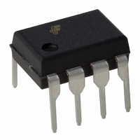
FAN7528N Fairchild Semiconductor, FAN7528N Datasheet - Page 13

FAN7528N
Manufacturer Part Number
FAN7528N
Description
IC PFC CTRLR CRM/TRANSITION 8DIP
Manufacturer
Fairchild Semiconductor
Datasheet
1.FAN7528MX.pdf
(21 pages)
Specifications of FAN7528N
Mode
Critical Conduction (CRM), Discontinuous (Transition)
Current - Startup
40µA
Voltage - Supply
12 V ~ 23 V
Operating Temperature
-40°C ~ 125°C
Mounting Type
Through Hole
Package / Case
8-DIP (0.300", 7.62mm)
Maximum Operating Temperature
+ 125 C
Mounting Style
Through Hole
Minimum Operating Temperature
- 40 C
Lead Free Status / RoHS Status
Lead free / RoHS Compliant
Frequency - Switching
-
Lead Free Status / Rohs Status
Lead free / RoHS Compliant
Available stocks
Company
Part Number
Manufacturer
Quantity
Price
Company:
Part Number:
FAN7528N
Manufacturer:
FSC
Quantity:
4 392
Part Number:
FAN7528N
Manufacturer:
FAIRCHILD/仙童
Quantity:
20 000
FAN7528 Rev. 1.0.6
© 2005 Fairchild Semiconductor Corporation
Applications Information
1. Error Amplifier Block
The error amplifier block has several functions, such as
dual output function, over-voltage protection function,
and disable function.
1.1 Dual-Output Function
Unlike conventional CRM PFC controllers, the FAN7528
has the dual-output control function according to the AC
line voltage without sensing the rectified AC line voltage.
Because the output voltage of the boost converter is pro-
portional to the peak voltage of the input AC line voltage
before the boost converter starts switching, the INV pin
voltage represents the peak AC line voltage. When the
AC line is connected to the boost converter, V
starts to increase from zero voltage. If the V
reaches 8.5V, the dual-output reference generator com-
pares the INV pin voltage with 1.3V reference and, if the
INV pin voltage is lower than 1.3V, the dual-output refer-
ence generator sets the reference voltage of the error
amplifier to 1.5V. If the INV pin voltage is higher than
1.3V, the reference voltage is set to 2.5V. That means if
the output voltage of the boost converter is set to 400V at
high line, the output voltage is 240V (400V*1.5/2.5) at
low line. If the output voltage is set to 390V at high line,
the output voltage is 234V at low line. Because this block
does not need the input voltage sensing network, the
power loss and cost related with the sensing network
can be saved. The reference voltage of the error ampli-
fier is not reset until V
Error Amp
Figure 35. Error Amplifier Block
Disable
OVP
2
COMP
Gm
CC
Dual-Output
Reference
Generator
goes below 4.5V.
2.66V
0.45V
1.5V/2.5V
0.35V
FAN7528 Rev. 1.00
2.55V
1
INV
V
CC
CC
OUT
voltage
voltage
13
1.2 Over-Voltage Protection Function
The control speed of the PFC converter is very slow;
therefore, the over-voltage protection (OVP) of the out-
put voltage is very important. The FAN7528 provides a
precise OVP function that shuts down the drive circuit
when the INV pin voltage exceeds 2.66V and there is
0.11V hysteresis.
1.3 Disable Function
If the INV pin voltage is lower than 0.45V, most of the
internal block is disabled, the operating current is
reduced to be 65µA, and there is 0.1V hysteresis in the
comparator.
1.4 Error Amplifier
The error amplifier is a transconductance type amplifier.
The output current of the amplifier is proportional to the
voltage difference between the inverting input and the
non-inverting input of the amplifier. Some resistors and
capacitors should be connected to the error amplifier
output pin, the COMP pin, for the output voltage loop
compensation.
2. Zero Current Detection Block
The zero current detector (ZCD) generates the turn-on
signal of the MOSFET when the boost inductor current
reaches zero using an auxiliary winding coupled with the
inductor. If the voltage of the ZCD pin goes higher than
1.5V, the ZCD comparator waits until the voltage goes
below 1.4V. If the voltage goes below 1.4V, the zero cur-
rent detector turns on the MOSFET. The ZCD pin is pro-
tected internally by two clamps, 6.7V high clamp and
0.6V low clamp. The 160µs timer generates a MOSFET
turn-on signal if the drive output has been low for more
than 160µs from the falling edge of the drive output.
V
IN
Figure 36. Zero Current Detector Block
R
ZCD
ZCD
5
6.7V
1.4V
1.5V
Zero Current
Detector
FAN7528 Rev. 1.00
160μs
Timer
S
R
www.fairchildsemi.com
Q
Turn-on
Signal


