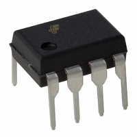
FAN6961DY Fairchild Semiconductor, FAN6961DY Datasheet - Page 9

FAN6961DY
Manufacturer Part Number
FAN6961DY
Description
IC PFC CONTROLLER DCM 8DIP
Manufacturer
Fairchild Semiconductor
Datasheet
1.FAN6961SZ.pdf
(13 pages)
Specifications of FAN6961DY
Mode
Discontinuous Conduction (DCM)
Frequency - Switching
60kHz
Current - Startup
10µA
Voltage - Supply
13.5 V ~ 24.5 V
Operating Temperature
-40°C ~ 125°C
Mounting Type
Through Hole
Package / Case
8-DIP (0.300", 7.62mm)
Lead Free Status / RoHS Status
Lead free / RoHS Compliant
© 2009 Fairchild Semiconductor Corporation
FAN6961 • Rev. 1.0.3
Functional Description
Error Amplifier
The inverting input of the error amplifier is referenced to
INV. The output of the error amplifier is referenced to
COMP. The non-inverting input is internally connected
to a fixed 2.5V ± 2% voltage. The output of the error
amplifier is used to determine the on-time of the PWM
output and regulate the output voltage. To achieve a
low input current THD, the variation of the on time
within one input AC cycle should be very small. A multi-
vector error amplifier is built in to provide fast transient
response and precise output voltage clamping.
For FAN6961, connecting a capacitance, such as 1µF,
between COMP and GND is suggested. The error
amplifier is a trans-conductance amplifier that converts
voltage to current with a 125µmho.
Startup Current
Typical startup current is less than 20µA. This ultra-low
startup current allows the usage of high resistance,
low-wattage startup resistor. For example, 1MΩ/0.25W
startup resistor and a 10µF/25V (V
are recommended for an AC-to-DC power adaptor with
a wide input range 85-265V
Operating Current
Operating current is typically 4.5mA. The low operating
current enables a better efficiency and reduces the
requirement of V
Maximum On-Time Operation
Given a fixed inductor value and maximum output
power, the relationship between on-time and line
voltage is:
If the line voltage is too low or the inductor value is too
high, t
frequency and achieve brownout protection, the
maximum value of t
R
R
The range of the maximum on-time is designed as 10 ~
50µs.
Peak Current Limiting
The switch current is sensed by one resistor. The
signal is feed into CS pin and an input terminal of a
comparator. A high voltage in CS pin terminates a
switching cycle immediately and cycle-by-cycle current
limit is achieved. The designed threshold of the
protection point is 0.82V.
t
t
I
I
on
on
, connected between MOT and GND. A 24kΩ resistor
generates corresponds to 25µs maximum on time:
(max)
=
V
2
ON
rms
•
=
L
2
is too long. To avoid extra low operating
R
•
•
P
I
(
η
o
k
Ω
CC
)
•
hold-up capacitance.
ON
25
24
is programmable by one resistor,
( )
μ
s
AC
.
CC
hold-up) capacitor
(1)
(2)
9
Leading-Edge Blanking (LEB)
A turn-on spike on CS pin appears when the power
MOSFET is switched on. At the beginning of each
switching pulse, the current-limit comparator is disabled
for around 400ns to avoid premature termination. The
gate drive output cannot be switched off during the
blanking period. Conventional RC filtering is not
necessary, so the propagation delay of current limit
protection can be minimized.
Under-Voltage Lockout (UVLO)
The turn-on and turn-off threshold voltage is fixed
internally at
guarantees a one-shot startup with proper startup
resistor and hold-up capacitor. With an ultra-low startup
current of 20µA, one 1MΩ R
under low input line voltage, 85V
on R
(V
Output Driver
With low on resistance and high current driving
capability, the output driver can drive an external
capacitive load larger than 3000pF. Cross conduction
current has been avoided to minimize heat dissipation,
improving efficiency and reliability. This output driver is
internally clamped by a 16.5V Zener diode.
Zero-Current Detection (ZCD)
The zero-current detection of the inductor is achieved
using its auxiliary winding. When the stored energy of
the inductor is fully released to output, the voltage on
ZCD goes down and a new switching cycle is enabled
after a ZCD trigger. The power MOSFET is always
turned on with zero inductor current such that turn-on
loss and noise can be minimized. The converter works
in boundary-mode and peak inductor current is always
exactly twice of the average current. A natural power
factor correction function is achieved with the low-
bandwidth, on-time modulation. An inherent maximum
off time is built in to ensure proper start-up operation.
This ZCD pin can be used as a synchronous input.
Noise Immunity
Noise on the current sense or control signal can cause
significant
boundary-mode operation. Slope compensation and
built-in debounce circuit can alleviate this problem.
Because the FAN6961 has a single ground pin, high
sink current at the output cannot be returned
separately. Good high-frequency or RF layout practices
should be followed. Avoiding long PCB traces and
component leads, locating compensation and filter
components near to the FAN6961, and increasing the
power MOSFET gate resistance improve performance.
AC
=265V
IN
would be less than 0.1W even under high line
rms
pulse-width
) condition.
12V/9.5V.
jitter,
This
IN
is sufficient for startup
rms
hysteresis behavior
particularly
. Power dissipation
www.fairchildsemi.com
in
the


