FDC6323L Fairchild Semiconductor, FDC6323L Datasheet
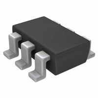
IC LOAD SWITCH INT 8VIN SSOT-6

FDC6323L

Manufacturer Part Number
FDC6323L
Description
IC LOAD SWITCH INT 8VIN SSOT-6
Manufacturer
Fairchild Semiconductor
Type
High Side Switchr
Datasheet

Specifications of FDC6323L

Number Of Outputs
1
Internal Switch(s)
Yes
Current Limit
1.5A
Voltage - Input
3 ~ 8 V
Operating Temperature
-55°C ~ 150°C
Mounting Type
Surface Mount
Package / Case
6-SSOT, SuperSOT-6
Configuration
Dual
Transistor Polarity
N and P-Channel
Power Dissipation
700 mW
Maximum Operating Temperature
+ 150 C
Mounting Style
SMD/SMT
Minimum Operating Temperature
- 55 C
Lead Free Status / RoHS Status
Lead free / RoHS Compliant
Rds (on)
-
Lead Free Status / Rohs Status
Lead free / RoHS Compliant
Other names
FDC6323L

Available stocks

Company
Part Number
Manufacturer
Quantity
Price
Part Number:
FDC6323L
Manufacturer:
FAIRCH
Quantity:
3 187
Part Number:
FDC6323L
Manufacturer:
FAIRCHILD/仙童
Quantity:
20 000
Part Number:
FDC6323L
0
Company:
Part Number:
FDC6323L
Quantity:
15 000
Symbol
V
V
I
P
T
ESD
THERMAL CHARACTERISTICS
R
R
© 1999 Fairchild Semiconductor Corporation
Absolute Maximum Ratings
L
General Description
J
IN
ON/OFF
D
These Integrated Load Switches are produced using
Fairchild's proprietary, high cell density, DMOS
technology. This very high density process is
especially tailored to minimize on-state resistance and
provide
devices are particularly suited for low voltage high
side load switch application where low conduction loss
and ease of driving are needed.
Integrated Load Switch
,T
FDC6323L
JA
JC
SuperSOT -6
STG
SOT-23
Parameter
Input Voltage Range
On/Off Voltage Range
Load Current @ V
Maximum Power Dissipation
Operating and Storage Temperature Range
Electrostatic Discharge Rating MIL-STD-883D Human Body
Model (100pf/1500Ohm)
Thermal Resistance, Junction-to-Ambient
Thermal Resistance, Junction-to-Case
superior
pin 1
TM
switching
SuperSOT
DROP
=0.5V - Continuous
performance.
TM
-6
- Pulsed
T
A
= 25°C unless otherwise noted
SuperSOT
O N / O FF
V i n , R 1
R 1 , C 1
These
(Note 1)
(Note 2a)
(Note 2)
(Note 1 & 3)
(Note 2a)
TM
4
5
6
-8
S e e A p p l i c a t i o n C i r c u i t
Features
Q 2
V
V
High density cell design for extremely low on-resistance.
V
>6KV Human Body Model.
SuperSOT
for superior thermal and electrical capabilities.
DROP
DROP
ON/OFF
Q 1
SO-8
=0.2V @ V
=0.3V @ V
Zener protection for ESD ruggedness.
3
2
1
TM
-6 package design using copper lead frame
V o u t , C 1
V o u t , C 1
R 2
IN
IN
=5V, I
=3.3V, I
FDC6323L
-55 to 150
1.5 - 8
SOT-223
3 - 8
180
1.5
2.5
0.7
60
6
L
IN
=1A, V
L
=1A, V
O N / O FF
ON/OFF
E Q U I V A L E N T C I R C U I T
ON/OFF
= 1.5V to 8V
+
V
= 1.5V to 8V.
D R O P
-
March 1999
SOIC-16
FDC6323L Rev.F
°C/W
°C/W
Units
kV
°C
W
V
V
A
O U T

Related parts for FDC6323L

FDC6323L Summary of contents

Page 1

... March 1999 =5V, I =1A 1. ON/OFF =3.3V, I =1A 1. ON/OFF Zener protection for ESD ruggedness package design using copper lead frame SOIC-16 SOT-223 FDC6323L 1 1.5 2.5 0.7 -55 to 150 6 180 Units °C kV °C/W °C/W FDC6323L Rev.F ...

Page 2

... Scale letter size paper 3. Pulse Test: Pulse Width < 300µs, Duty Cycle < 2.0% = 25°C unless otherwise noted) Conditions ON/OFF ON/OFF 3 ON/OFF ON/OFF DROP IN ON/OFF DROP IN ON/OFF J Min Typ Max 3 1.5 0.145 0.2 0.178 0 Units 1 µA -1 µ guaranteed JC FDC6323L Rev.F ...

Page 3

... 1 ON/OFF 0.1 PW =300us Figure 2. V =5V ON/OFF 0.35 PW =300us 0.3 0.25 0.2 0.15 0 Figure 4. R =1A 1 ON/OFF PW =300us 125° 25° 3. 1 ON/OFF PW =300us (A) L Versus =3.3V. DROP 3.3V PW =300us 125° 25° ,(A) L Versus =3.3V. (ON FDC6323L Rev ...

Page 4

... Vin=3.3V and R1=20KOhm. 250 Vin = 5V 200 150 tr 100 tf 3.3V td(off) 50 td(on) 2. Figure Current Overshoot Variation with Vin and R2 d(on) 3.3V V OUT 10 50% IN 10% 80 100 Figure 11. Switching Waveforms. Vin = 3. Von/off = 3. 20K td(off td(on Von/off = 3. 20K off d(off 90% 90% 10% INVERTED 90% 50% PULSE W IDTH FDC6323L Rev.F ...

Page 5

... Figure 13. Transient Thermal Response Curve. Note: Thermal characterization performed on the conditions described in Note 2a. Transient thermal response will change depends on the circuit board design unless otherwise noted ) 0.01 0 TIME (sec ( See Note 2a JA P(pk ( Duty Cycle 100 300 FDC6323L Rev.F ...

Page 6

... FDC6323L Load Switch Application APPLICATION CIRCUIT Component Values R1 Typical 10k - 1M R2 Typical 0 - 100k C1 Typical 1000pF Design Notes R1 is needed to turn off Q2. R2 can be used to soft start the switch in case the output capacitance Co is small. R2 should be at least 10 times smaller than R1 to guarantee Q1 turns on. ...

Page 7

... TRADEMARKS The following are registered and unregistered trademarks Fairchild Semiconductor owns or is authorized to use and is not intended exhaustive list of all such trademarks. ACEx™ CoolFET™ CROSSVOLT™ CMOS FACT™ FACT Quiet Series™ ® FAST FASTr™ GTO™ ...

Related keywords