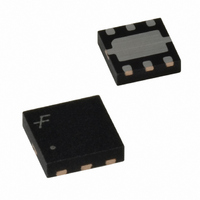
FPF2174 Fairchild Semiconductor, FPF2174 Datasheet

FPF2174
Specifications of FPF2174
Related parts for FPF2174
FPF2174 Summary of contents
Page 1
... FPF2174 200 ©2008 Fairchild Semiconductor Corporation FPF2174 Rev. F General Description The FPF2174 is a load switch which combines the functionality TM of the IntelliMAX series load switch with a very low forward voltage drop Schottky barrier rectifier and a zener clamp at the output. The integrated solution provides full protection to systems and loads which may encounter large current conditions in a very compact MLP 3x3 package ...
Page 2
... Pin Description Pin Name OUT 4 GND 5 FLAGB PAD1 FPF2174 Rev. F CONTROL LOGIC CURRENT LIMIT 3x3 MLP BOTTOM VIEW Function Supply Input: Input to the power switch and the supply voltage for the IC No Connect Switch Output: Output of the power switch Ground Fault Output: Active LO, open drain output which indicates an over current supply, under voltage or over temperature state ...
Page 3
... Reverse Block Leakage Current Reverse Breakdown Voltage Dropout Voltage ON Input Logic High Voltage (ON) ON Input Logic Low Voltage ON Input Leakage Off Switch Leakage FLAGB Output Logic Low Voltage FLAGB Output High Leakage Current FPF2174 Rev. F HBM MM Symbol Conditions 0mA V = 1.8 to 3.3V OUT IN ...
Page 4
... Delay On Time Delay Off Time V Rise Time OUT V Fall Time OUT Over Current Blanking Time Short Circuit Response Time Note 1: Package power dissipation on 1 square inch pad, 2 oz. copper board. FPF2174 Rev. F Symbol Conditions 3.3V LIM IN Shutdown Threshold Return from Shutdown Hysteresis ...
Page 5
... V 0.6 0.4 0.2 0.0 -40 - JUNCTION TEMPERATURE J Figure 3. I Current vs. Temperature SHUTDOWN 3. -40 - JUNCTION TEMPERATURE J Figure 5. Latchoff current vs. Temperature FPF2174 Rev. F 120 110 100 4.5 5.0 5.5 6.0 0.6 0.5 0.4 0.3 = 5.5V 0 3. 1.8 1.6 1 ...
Page 6
... V , INPUT VOLTAGE (V) IN Figure 9. Drop Voltage vs. Input Voltage 16.0 15.9 15.8 15.7 15.6 15.5 15 ZENER CURRENT (mA) Figure 11. Zener Voltage vs. Zener Current FPF2174 Rev. F 400 350 300 250 200 -40 500 450 400 350 300 250 200 150 100 - Figure 10. Drop Voltage vs. Temperature ...
Page 7
... Figure 13. Single Pulse Maximum Power Dissipation of Zener Diode 1000 t T FALL FALL 100 t T RISE RISE 10 1 -40 - JUNCTION TEMPERATURE J Figure 15 vs. Temperature Rise Fall V DRV 2V/DIV V FLAGB C 2V/DIV C I OUT 200mA/DIV V OUT 2V/DIV 5ms/DIV Figure 17. T Response BLANK FPF2174 Rev - 0.001 2V/DIV = 0 OUT 10mA/DIV 7 ...
Page 8
... Typical Characteristics V ON 2V/DIV I OUT 10mA/DIV 200ns/DIV Figure 19. T Response OFF V IN 2V/DIV I OUT 200mA/DIV 50 s/DIV Figure 21. Current Limit Response Time (Switch power up to hard short) FPF2174 Rev 3. 0 OUT R = 500 L 2V/DIV I OUT 5A/DIV V IN 2V/DIV Figure 20. Short Circuit Response Time ...
Page 9
... Description of Operation The FPF2174 is a current limited switch that protects systems and loads which can be damaged or disrupted by the application of high currents. The core of the device is a 0.125 P-channel MOSFET and a controller capable of functioning over a wide input operating range of 1.8-5.5V paired with a low forward voltage drop Schottky diode for reverse blocking and a 16V zener diode for output clamp ...
Page 10
... To be most effective, the input and output capacitors should be placed close to the device to minimize the effects that parasitic trace inductances may have on normal and short-circuit operation. Using wide traces for V IN minimize parasitic electrical effects along with minimizing the case to ambient thermal impedance. FPF2174 Rev OUT FPF2174 ON ...
Page 11
... Dimensional Outline and Pad Layout FPF2174 Rev. F Package MLP06H 11 www.fairchildsemi.com ...
Page 12
... PRODUCT STATUS DEFINITIONS Definition of Terms Datasheet Identification Product Status Advance Information Formative / In Design Preliminary First Production No Identification Needed Full Production Obsolete Not In Production FPF2174 Rev. F F-PFS™ PowerTrench ® FRFET Programmable Active Droop™ SM ® Global Power Resource QFET Green FPS™ QS™ ...


