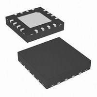
ISL6269CRZ Intersil, ISL6269CRZ Datasheet - Page 13

ISL6269CRZ
Manufacturer Part Number
ISL6269CRZ
Description
IC CTRLR PWM 1-PHASE GPU 16-QFN
Manufacturer
Intersil
Datasheet
1.ISL6269CRZ.pdf
(14 pages)
Specifications of ISL6269CRZ
Pwm Type
Controller
Number Of Outputs
1
Frequency - Max
600kHz
Voltage - Supply
7 V ~ 25 V
Buck
Yes
Boost
No
Flyback
No
Inverting
No
Doubler
No
Divider
No
Cuk
No
Isolated
No
Operating Temperature
-10°C ~ 100°C
Package / Case
16-VQFN Exposed Pad, 16-HVQFN, 16-SQFN, 16-DHVQFN
Frequency-max
600kHz
Lead Free Status / RoHS Status
Lead free / RoHS Compliant
Duty Cycle
-
Available stocks
Company
Part Number
Manufacturer
Quantity
Price
Company:
Part Number:
ISL6269CRZ
Manufacturer:
INTERSIL
Quantity:
17
Part Number:
ISL6269CRZ
Manufacturer:
INTERSIL
Quantity:
20 000
Part Number:
ISL6269CRZ-T
Manufacturer:
INTERSIL
Quantity:
20 000
FCCM (PIN 3), EN (PIN 4), AND PGOOD (PIN 16)
These are logic inputs that are referenced to the GND pin.
Treat as a typical logic signal.
COMP (PIN 5), FB (PIN 6), AND VO (PIN 8)
For best results, use an isolated sense line from the output
load to the VO pin. The input impedance of the FB pin is
high, so place the voltage programming and loop
compensation components close to the VO, FB, and GND
pins keeping the high impedance trace short.
FSET (PIN 7)
This pin requires a quiet environment. The resistor R
and capacitor C
this pin. Keep fast moving nodes away from this pin.
ISEN (PIN 9)
Route the connection to the ISEN pin away from the traces
and components connected to the FB pin, COMP pin, and
FSET pin.
Intersil products are sold by description only. Intersil Corporation reserves the right to make changes in circuit design, software and/or specifications at any time without
notice. Accordingly, the reader is cautioned to verify that data sheets are current before placing orders. Information furnished by Intersil is believed to be accurate and
reliable. However, no responsibility is assumed by Intersil or its subsidiaries for its use; nor for any infringements of patents or other rights of third parties which may result
from its use. No license is granted by implication or otherwise under any patent or patent rights of Intersil or its subsidiaries.
All Intersil U.S. products are manufactured, assembled and tested utilizing ISO9000 quality systems.
FSET
Intersil Corporation’s quality certifications can be viewed at www.intersil.com/design/quality
should be placed directly adjacent to
For information regarding Intersil Corporation and its products, see www.intersil.com
13
FSET
ISL6269
LG (PIN 11)
The signal going through this trace is both high dv/dt and
high di/dt, with high peak charging and discharging current.
Route this trace in parallel with the trace from the PGND pin.
These two traces should be short, wide, and away from
other traces. There should be no other weak signal traces in
proximity with these traces on any layer.
BOOT (PIN 13), UG (PIN 14), AND PHASE (PIN 15)
The signals going through these traces are both high dv/dt
and high di/dt, with high peak charging and discharging
current. Route the UG and PHASE pins in parallel with short
and wide traces. There should be no other weak signal
traces in proximity with these traces on any layer.
Copper Size for the Phase Node
The parasitic capacitance and parasitic inductance of the
phase node should be kept very low to minimize ringing. It is
best to limit the size of the PHASE node copper in strict
accordance with the current and thermal management of the
application. An MLCC should be connected directly across
the drain of the upper MOSFET and the source of the lower
MOSFET to suppress the turn-off voltage spike.
June 25, 2009
FN9177.3


