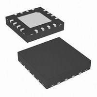
ISL6269CRZ Intersil, ISL6269CRZ Datasheet - Page 7

ISL6269CRZ
Manufacturer Part Number
ISL6269CRZ
Description
IC CTRLR PWM 1-PHASE GPU 16-QFN
Manufacturer
Intersil
Datasheet
1.ISL6269CRZ.pdf
(14 pages)
Specifications of ISL6269CRZ
Pwm Type
Controller
Number Of Outputs
1
Frequency - Max
600kHz
Voltage - Supply
7 V ~ 25 V
Buck
Yes
Boost
No
Flyback
No
Inverting
No
Doubler
No
Divider
No
Cuk
No
Isolated
No
Operating Temperature
-10°C ~ 100°C
Package / Case
16-VQFN Exposed Pad, 16-HVQFN, 16-SQFN, 16-DHVQFN
Frequency-max
600kHz
Lead Free Status / RoHS Status
Lead free / RoHS Compliant
Duty Cycle
-
Available stocks
Company
Part Number
Manufacturer
Quantity
Price
Company:
Part Number:
ISL6269CRZ
Manufacturer:
INTERSIL
Quantity:
17
Part Number:
ISL6269CRZ
Manufacturer:
INTERSIL
Quantity:
20 000
Part Number:
ISL6269CRZ-T
Manufacturer:
INTERSIL
Quantity:
20 000
LG (Pin 11)
The LG pin is the output of the low-side MOSFET gate
driver. Connect to the gate of the low-side MOSFET.
PVCC (Pin 12)
The PVCC pin is the input voltage bias for the LG low-side
MOSFET gate driver. Connect +5V from the PVCC pin to the
PGND pin. Decouple with at least 1µF of an MLCC capacitor
across the PVCC and PGND pins. The VCC output may be
used for the PVCC input voltage source.
BOOT (Pin 13)
The BOOT pin stores the input voltage for the UG high-side
MOSFET gate driver. Connect an MLCC capacitor across
the BOOT and PHASE pins. The boot capacitor is charged
through an internal boot diode connected from the PVCC pin
to the BOOT pin, each time the PHASE pin drops below
PVCC minus the voltage dropped across the internal boot
diode.
UG (Pin 14)
The UG pin is the output of the high-side MOSFET gate
driver. Connect to the gate of the high-side MOSFET.
PHASE (Pin 15)
The PHASE pin detects the voltage polarity of the PHASE
node and is also the current return path for the UG high-side
MOSFET gate driver. Connect the PHASE pin to the node
consisting of the high-side MOSFET source, the low-side
MOSFET drain, and the output inductor.
PGOOD (Pin 16)
The PGOOD pin is an open-drain output that indicates when
the converter is able to supply regulated voltage. Connect
the PGOOD pin to +5V through a pull-up resistor.
GND (Bottom Pad)
Signal common of the IC. Unless otherwise stated, signals
are referenced to the GND pin, not the PGND pin.
Theory of Operation
Modulator
The ISL6269 is a hybrid of fixed frequency PWM control, and
variable frequency hysteretic control. Intersil’s R
can simultaneously affect the PWM switching frequency and
PWM duty cycle in response to input voltage and output load
transients. The term “Ripple” in the name “Robust-Ripple-
Regulator” refers to the converter output inductor ripple
current, not the converter output ripple voltage. The R
modulator synthesizes an AC signal V
representation of the output inductor ripple current. The
duty-cycle of V
current through a ripple capacitor C
C
R
is provided by a transconductance amplifier g
R
is the result of charge and discharge
7
R
. The current through
R
, which is an ideal
3
technology
m
that
3
ISL6269
measures the VIN and VO pin voltages. The positive slope
of V
The negative slope of V
Where g
A window voltage V
amplifier output voltage V
which the ripple voltage V
V
pins. The V
comparator in which V
and V
PWM pulses being generated as V
V
proportional to the slew rates of the positive and negative
slopes of V
proportional to the voltage between V
EN, LDO, and POR
The VCC LDO regulates by pulling up towards the voltage at
the VIN pin; the LDO has no pull-down capability. The LDO
is enabled when the EN pin surpasses the rising EN threshold
voltage V
increased above the rising power-on reset (POR)
threshold voltage. The controller immediately stops
generating PWM and disables the LDO when the EN pin is
pulled below the falling EN threshold voltage V
completely shuts off when
POR
Soft-Start, and PGOOD
The ISL6269 uses a digital soft-start circuit to ramp the
output voltage of the converter to the programmed regulation
setpoint at a predictable slew rate. The slew rate of the
soft-start sequence has been selected to limit the inrush
current through the output capacitors as they charge to the
V
V
W
COMP
RPOS
RNEG
Ripple Capacitor Voltage C R
FIGURE 3. MODULATOR WAVEFORMS DURING LOAD
R
is set by a resistor connected across the FSET and GND
V
W
can be written as:
VCC_THF
=
=
thresholds . The PWM switching frequency is
m
is the higher threshold voltage. Figure 3 shows
ENTHR
(
g
is the gain of the transconductance amplifier.
g
R;
m
R,
m
⋅
TRANSIENT
) V
the PWM switching frequency is inversely
V
V
•
COMP,
(
threshold voltage.
OUT
. The ISL6269 is enabled once
IN
W
–
V
is referenced with respect to the error
COMP
and V
OUT
R
COMP
R
can be written as:
V
)
is compared. The amplitude of
VCC
W
is the lower threshold voltage
signals feed into a window
Error Amplifier Voltage V COMP
, creating an envelope into
decreases below the falling
R
Window Voltage V W
traverses the V
W
and V
PWM
ENTHF
COMP.
V
VCC
V
June 25, 2009
VCC_THR
. The IC
W
has
FN9177.3
(EQ. 1)
(EQ. 2)
and


