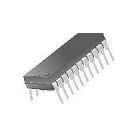
FAN7585SN Fairchild Semiconductor, FAN7585SN Datasheet

FAN7585SN
Specifications of FAN7585SN
Related parts for FAN7585SN
FAN7585SN Summary of contents
Page 1
... Power Good Signal Generator with Hysteresis Typical Application • PC Power Supply 24-SDIP 1 ©2003 Fairchild Semiconductor Corporation www.fairchildsemi.com Description The FAN7585 is a fixed frequency improved performance pulse width modulation control circuit with complete house- keeping circuitry for use in the secondary side of SMPS (Switched Mode Power Supply) ...
Page 2
FAN7585 Internal Block Diagram OSCILLATOR T T COMP 2 E/A(-) 3 E/A(+) 4 1.25V DTC 21 INTERNAL BIAS Vref 12 Vref Start Up Vcc DET 9 COMP2 PWM CONTROL CK ...
Page 3
Pin Definition C1 GND Vcc COMP E/A(-) E/A(+) T Pin Description Pin Pin I/O Pin Function Description Number Name Supply Voltage CC 2 COMP O E/A Output 3 E/A(-) I E/A (-) Input ...
Page 4
FAN7585 Pin Function Pin Number Pin Name 1 V Supply voltage. Operating range is 15V~30V. Test condition : V CC Error amplifier output connected to non-inverting input of pulse width modulator 2 COMP comparator. 3 E/A(-) Error amplifier ...
Page 5
Absolute Maximum Ratings Characteristics Supply Voltage Collector Output Voltage Collector Output Current Power Dissipation (FAN7585) Operating Temperature Range Storage Temperature Range Temperature Characteristics Characteristics Temperature Coefficient of Vref (-25°C ≤ Ta ≤ 85°C) Symbol Value ...
Page 6
FAN7585 Electrical Characteristics (V =20V, T =25°C, unless otherwise specified Parameter REFERENCE SECTION Reference Output Voltage Line Regulation Load Regulation Temperature Coefficient of Vref Short Circuit Output Current OSCILLATOR SECTION Oscillation Frequency Frequency Change with Temperature DEAD TIME ...
Page 7
Electrical Characteristics (V =20V, T =25°C, unless otherwise specified Parameter PROTECTION SECTION Over Voltage Protection for +3.3V Over Voltage Protection for +5V Over Voltage Protection for +12V Input Threshold Voltage for PT Under Voltage Protection for +3.3V Under ...
Page 8
FAN7585 Application Informations 100 10 1 0.2 2 Rt/Ct Feedback Dead-time control Output Q1 Output Q2 8 Timing Resistance vs Frequency CT=1nF CT=2.2nF CT=4.7nF CT=10nF CT=20nF CT=50nF CT=100nF ...
Page 9
OVP Block Vo R101 PT D R102 The OVP function is simply realized by connecting Pin14, Pin16, Pin18 to each secondary outputs. R1, R2, R3, R4, R5, R6 are internal resistors of the IC. Each OVP level is determined ...
Page 10
FAN7585 2. UVP Block The block is made comparator with three detecting inputs and without hysteresis voltage. Each UVP level is determined by resistor ratio and the typical values are 2.3V/4.0V/10V respectively. • UVP detecting voltage for ...
Page 11
OCP Block Sense Inductor Equivalent Resistor(Rs) ≅ 5mΩ Io (Offset Voltage Resistor) It also has OCP function for +3.3V,+5V,+12V outputs. The block is made up of three comparators. Pin17(IS12), pin15(IS5) and pin13(IS33) are current sense inputs for +12V, +5V ...
Page 12
FAN7585 4. Remote On/Off & Delay Block 5V Rpull 1.25V 6 REM Remote On/Off Remote On/Off section is controlled by a microprocessor high signal is supplied to the Remote On/Off input(Pin6), the output of COMP6 becomes high status. ...
Page 13
Power Good Signal Generator Vcc 60kΩ DET 9 R12 4.7kΩ Power Good Signal Generator circuit generates "ON or OFF" signal depending on the status of output voltage to prevent the malfunctions of following systems like microprocessor, etc. caused by ...
Page 14
FAN7585 Typical Application Circuit FAN7585 1 Vcc C1 2 COMP GND 3 EA(-) C2 C22 4 EA(+) DTC C21 PSON REM(PSON) PT C20 7 Rt/Ct V12 R47 8 RI IS12 9 DET V5 C19 ...
Page 15
Mechanical Dimensions Package Dimensions in millimeters 24-SDIP FAN7585 15 ...
Page 16
... FAN7585 24-SDIP DISCLAIMER FAIRCHILD SEMICONDUCTOR RESERVES THE RIGHT TO MAKE CHANGES WITHOUT FURTHER NOTICE TO ANY PRODUCTS HEREIN TO IMPROVE RELIABILITY, FUNCTION OR DESIGN. FAIRCHILD DOES NOT ASSUME ANY LIABILITY ARISING OUT OF THE APPLICATION OR USE OF ANY PRODUCT OR CIRCUIT DESCRIBED HEREIN; NEITHER DOES IT CONVEY ANY LICENSE UNDER ITS PATENT RIGHTS, NOR THE RIGHTS OF OTHERS. ...


