RC1585MT Fairchild Semiconductor, RC1585MT Datasheet - Page 6
RC1585MT
Manufacturer Part Number
RC1585MT
Description
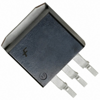
IC REG LDO ADJ 5A TO-263
Manufacturer
Fairchild Semiconductor
Datasheet
1.RC1585M15.pdf
(12 pages)
Specifications of RC1585MT
Applications
Converter, Pentium® II GTL+, Pro
Voltage - Input
3.5 ~ 7 V
Number Of Outputs
1
Voltage - Output
1.5 ~ 3.6 V
Operating Temperature
0°C ~ 125°C
Mounting Type
Surface Mount
Package / Case
D²Pak, TO-263 (3 leads + tab)
Lead Free Status / RoHS Status
Contains lead / RoHS non-compliant
Other names
RC1585MTTR
Available stocks
Company
Part Number
Manufacturer
Quantity
Price
Company:

Part Number:
RC1585MT
Manufacturer:
FAIRCHILD
Quantity:
1 250
Part Number:
RC1585MT
Manufacturer:
FAIRCHILD/仙童
Quantity:
20 000


General
The RC1585 and RC1585-1.5 are three-terminal regulators
optimized for GTL+ V
applications. These devices are short-circuit protected, safe
area protected, and offer thermal shutdown to turn off the
regulator when the junction temperature exceeds about
150 C. The RC1585 series provides low dropout voltage
and fast transient response. Frequency compensation uses
capacitors with low ESR while still maintaining stability.
This is critical in addressing the needs of low voltage high
speed microprocessor buses like GTL+.
Stability
The RC1585 series requires an output capacitor as a part
of the frequency compensation. It is recommended to use a
22 F solid tantalum or a 100 F aluminum electrolytic on
the output to ensure stability. The frequency compensation
of these devices optimizes the frequency response with low
ESR capacitors. In general, it is suggested to use
capacitors with an ESR of 1 . It is also recommended to
use bypass capacitors such as a 22 F tantalum or a 100 F
aluminum on the adjust pin of the RC1585 for low ripple
and fast transient response. When these bypassing
capacitors are not used at the adjust pin, smaller values of
output capacitors provide equally good results.
Protection Diodes
In normal operation, the RC1585 series does not require
any protection diodes. For the RC1585, internal resistors
limit internal current paths on the adjust pin. Therefore,
even with bypass capacitors on the adjust pin, no
protection diode is needed to ensure device safety under
short-circuit conditions.
A protection diode between the input and output pins is
usually not needed. An internal diode between the input
and the output pins on the RC1585 series can handle
microsecond surge currents of 50A to 100A. Even with
large value output capacitors it is difficult to obtain those
values of surge currents in normal operation. Only with
large values of output capacitance, such as 1000 F to
5000 F, and with the input pin instantaneously shorted to
ground can damage occur. A crowbar circuit at the input
can generate those levels of current; a diode from output to
input is then recommended, as shown in Figure 10.
Usually, normal power supply cycling or system “hot
plugging and unplugging” will not generate current large
enough to do any damage.
RC1585
SPECIFICATION
Applications Information
6
TT
termination and logic
V
IN
Ripple Rejection
In applications that require improved ripple rejection, a
bypass capacitor from the adjust pin of the RC1585 to
ground reduces the output ripple by the ratio of
V
the ripple frequency should be less than the value of R1
(typically in the range of 100 to 120 ) in the feedback
divider network in Figure 10. Therefore, the value of the
required adjust pin capacitor is a function of the input
ripple frequency. For example, if R1 equals 100 and
the ripple frequency equals 120Hz, the adjust pin
capacitor should be 22 F. At 10kHz, only 0.22 F is
needed.
Output Voltage
The RC1585 regulator develops a 1.25V reference
voltage between the output pin and the adjust pin (see
Figure 11). Placing a resistor R1 between these two
terminals causes a constant current to flow through R1
and down through R2 to set the overall output voltage.
Normally, this current is the specified minimum load
current of 10mA.
V
OUT
The adjust pin can be driven on a transient basis 7V
with respect to the output, without any device
degradation. As with any IC regulator, exceeding the
maximum input-to-output voltage differential causes
the internal transistors to break down and none of the
protection circuitry is then functional.
IN
C1
10 F
/1.25V. The impedance of the adjust pin capacitor at
C1
10 F
+
+
Figure 10. Optional Protection
IN
(OPTIONAL)
IN
(OPTIONAL)
RC1585-1.5
1N4002
RC1585
PRODUCT
1N4002
+
ADJ
D1
GND
D1
OUT
C
OUT
ADJ
+
R1
R2
C2
22 F
+
C2
22 F
V
OUT
V
OUT
Related parts for RC1585MT
Image
Part Number
Description
Manufacturer
Datasheet
Request
R

Part Number:
Description:
Manufacturer:
Fairchild Semiconductor
Datasheet:
Part Number:
Description:
Fairchild Semiconductor [IGBT MODULE]
Manufacturer:
Fairchild Semiconductor
Datasheet:

Part Number:
Description:
Discrete Semiconductor Modules
Manufacturer:
Fairchild Semiconductor
Part Number:
Description:
Discrete Semiconductor Modules
Manufacturer:
Fairchild Semiconductor
Part Number:
Description:
This N-Channel MOSFET is produced using Fairchild Semiconductor’s advanced Power Trench® process
Manufacturer:
Fairchild Semiconductor
Datasheet:
Part Number:
Description:
This N-Channel MOSFET is produced using Fairchild Semiconductor’s advanced Power Trench® process
Manufacturer:
Fairchild Semiconductor
Datasheet:
Part Number:
Description:
This N-Channel MOSFET is produced using Fairchild Semiconductor’s advanced PowerTrench® process
Manufacturer:
Fairchild Semiconductor
Datasheet:
Part Number:
Description:
This N-Channel MOSFET is produced using Fairchild Semiconductor’s advanced PowerTrench® process
Manufacturer:
Fairchild Semiconductor
Datasheet:
Part Number:
Description:
This N-Channel MOSFET is produced using Fairchild Semiconductor’s advanced Power Trench® process
Manufacturer:
Fairchild Semiconductor
Datasheet:
Part Number:
Description:
This N-Channel logic Level MOSFETs are produced using Fairchild Semiconductor‘s advanced Power Trench® process that has been special tailored to minimize the on-state resistance and yet maintain superior switching performance
Manufacturer:
Fairchild Semiconductor
Datasheet:
Part Number:
Description:
This N-Channel MOSFET is produced using Fairchild Semiconductor’s advanced Power Trench® process
Manufacturer:
Fairchild Semiconductor
Datasheet:
Part Number:
Description:
This N-Channel SyncFET™ is produced using Fairchild Semiconductor’s advanced PowerTrench® process
Manufacturer:
Fairchild Semiconductor
Datasheet:
Part Number:
Description:
This N-Channel SyncFET™ is produced using Fairchild Semiconductor’s advanced PowerTrench® process
Manufacturer:
Fairchild Semiconductor
Datasheet:
Part Number:
Description:
This N-Channel SyncFET™ is produced using Fairchild Semiconductor’s advanced PowerTrench® process
Manufacturer:
Fairchild Semiconductor
Datasheet:
Part Number:
Description:
This N-Channel logic Level MOSFETs are produced using Fairchild Semiconductor‘s advanced Power Trench® process that has been special tailored to minimize the on-state resistance and yet maintain superior switching performance
Manufacturer:
Fairchild Semiconductor
Datasheet: