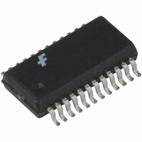
FAN5235QSC Fairchild Semiconductor, FAN5235QSC Datasheet - Page 8

FAN5235QSC
Manufacturer Part Number
FAN5235QSC
Description
IC CTRLR DC/DC MOBILE PC 24QSOP
Manufacturer
Fairchild Semiconductor
Datasheet
1.FAN5235QSCX.pdf
(15 pages)
Specifications of FAN5235QSC
Applications
Converter, Mobile PCs
Voltage - Input
5.4 ~ 24 V
Number Of Outputs
5
Voltage - Output
3.3V, 5V, 12V
Operating Temperature
-20°C ~ 85°C
Mounting Type
Surface Mount
Package / Case
24-QSOP
Output Voltage
3.3 V, 5 V
Output Current
50 mA
Input Voltage
5.4 V to 24 V
Mounting Style
SMD/SMT
Maximum Operating Temperature
+ 85 C
Minimum Operating Temperature
- 20 C
Lead Free Status / RoHS Status
Lead free / RoHS Compliant
Other names
FAN5235QSC_NL
FAN5235QSC_NL
FAN5235QSC_NL
Available stocks
Company
Part Number
Manufacturer
Quantity
Price
Part Number:
FAN5235QSC
Manufacturer:
FAIRCHILD/仙童
Quantity:
20 000
Part Number:
FAN5235QSCX
Manufacturer:
FAIRCHILD/仙童
Quantity:
20 000
REV. 1.3.3 1/3/02
Peak current is DC output current plus peak ripple current:
where T is the maximum period, V
is the inductance. This current generates a voltage on the
low-side MOSFET of 7A • 20m = 140mV. The current
limit threshold is typically 150mV (worst-case 135mV) with
R2 = 1K , and so this value is suitable. R2 could be
increased a further 10% if additional noise margin is deemed
necessary.
Precision Current Limit
Precision current limiting can be achieved by placing a
discrete sense resistor between the source of the low-side
MOSFET and ground.
In this case, current limit accuracy is set by the tolerance of
the IC, +10%.
Shutdown (SDWN)
The SDWN pin turns off all 5 converters (+5V, +3.3V, and
+12V, 5V/3.3V-ALWAYS) and puts the FAN5235 into a low-
power mode (Shutdown mode).
This mode of operation implies the use of a push button
switch between SDWN and Vin. Pushing the button allows
(for the duration of the contact) to power the 3.3V-ALWAYS
and 5V-ALWAYS long enough for the uC to power up and in
turn latch the SDWN pin high.
Once the SDWN is high then the ALWAYS voltages are
enabled to go high if the respective SDN3.3 and SDN5 go
high.
MAIN 3.3V and 5V Softstart, Sequencing and
Stand-by
Softstart of the 3.3V and 5V converters is accomplished by
means of an external capacitor between pins SDN3.3 (SDN5)
and ground.
I
pk
Figure 4. Using a Precision Current Sense Resistor
I
dc
+
TV
2L
ISEN
GND
HSD
LSD
SW
0
= 5A +
4µsec • 5V
2 • 5µH
O
is output voltage, and L
= 7A
The 3.3V (5V) main converter is turned ON if SDWN and
SDN3.3 (SDN5) are both high and is turned off if either SDWN
or SDN3.3 (SDN5) is low.
Stand-by mode is defined as the condition by which V-Mains
are OFF and V-ALWAYS are ON (SDWN=1 and
SDN3.3=SDN5=0).
ALWAYS mode of Operation
If it is desired that 5V-ALWAYS and 3.3V-ALWAYS are always
ON then the SDWN pin must be connected to Vin permanently.
This way the two ALWAYS regulators come up as soon as there
is power while the state of the Main regulators can be controlled
via the SDN5 and SDN3.3 pins.
Sequencing Table
3.3V Voltage Adjustment
The output voltage of the 3.3V converter can be increased by
as much as 10% by inserting a resistor divider in the feedback
line. The feedback pin impedance is about 66K . Thus, for
example, to increase the output of the 3.3V converter by 10%,
use a 2.21K /33.2K divider.
Note that the output of the 5V regulator cannot be adjusted.
The feedback line of the 5V regulator is used internally as a
5V supply and, therefore, cannot tolerate any impedance in
series with it.
3.3V and 5V Main Overvoltage Protection
(Soft Crowbar)
When the output voltage of the 3.3V (or the 5V) converter
exceeds approximately 115% of nominal, the converter enters
the over-voltage (OV) protection mode, with the goal of pro-
tecting the load from damage. During operation, severe load
dump or a short of an upper MOSFET could cause the output
voltage to increase significantly over normal operation range
without circuit protection. When the output exceeds the over-
voltage threshold, the over-voltage comparator forces the
lower gate driver high and turns the lower MOSFET on. This
will pull down the output voltage and eventually may blow the
battery fuse. As soon as output voltage drops below the thresh-
old, OVP comparator is disengaged.
The OVP scheme also provides a soft crowbar function
(bang-bang control followed by blow of the fuse) which
helps to tackle severe load transients but does not invert out-
put voltage when activated—a common problem for OVP
schemes with a latch. The prevention of output inversion
eliminates the need for a Schottky diode across the load.
SDN5
X
1
0
1
0
SDN3.3 SDWN
X
0
0
1
1
0
1
1
1
1
ALWAYS
3V&5V
0
1
1
1
1
MAIN
5V
0
0
1
0
1
FAN5235
MAIN
3.3V
0
0
0
1
1
8


