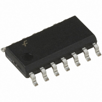
FAN1655M Fairchild Semiconductor, FAN1655M Datasheet

FAN1655M
Specifications of FAN1655M
Available stocks
Related parts for FAN1655M
FAN1655M Summary of contents
Page 1
... FAN1655 into a low power mode. The FAN1655 regulator is available in a power-enhanced eTSSOP™-16, standard SOIC-14, and an 8-Lead MLP package. Ordering Information Part Number FAN1655M FAN1655MX FAN1655MTF FAN1655MTFX FAN1655MPX Block Diagram VDDQ VREFOUT VREFIN VSSQ ©2006 Fairchild Semiconductor Corporation FAN1655 Rev. 1.1.5 Features bi-directional LDO Sinks and sources 2 ...
Page 2
... VTTFORCE 3 6 VTTFORCE VDD 4 5 GND 8-Lead MLP Package (5x6mm) = 4˚C/W, = 34˚C measured on FAN1655MP Eval Board Pin Name VDD Input power for the LDO. VTTFORCE The VTT output voltage. VSS IC Ground. 9 VTTSENSE Feedback for remote sense of the VTT voltage. 10 VREFIN Alternative input for direct control of VTTOUT and VREFOUT ...
Page 3
... SHDN VTTSENSE (connect to VTTFORCE 1nF at the load) GND V Output Change vs. I REF REF 2.5V DD DDQ T = 25˚ LOAD CURRENT (mA) REF Figure 3. Reference Output Load Regulation T =70° =25° 1.5 2 2.5 Peak Load Current (A) Current vs. Pulse Width (FAN1655M SO-14 Package) www.fairchildsemi.com ...
Page 4
... IDD Supply Current VDDQ Leakage Current VDD Leakage Current SHDN Input Current Over-Temperature Shutdown Over-Temperature Hysteresis FAN1655 Rev. 1.1.5 FAN1655M (SOIC-14) FAN1655MTF (e-TSSOP) FAN1655MP (MLP) Conditions = 25˚C using circuit in Figure 1, unless otherwise noted.) A Conditions I = 0A, VREFIN = open OUT VDDQ = 2.3V VDDQ = 2.5V VDDQ = 2 ...
Page 5
Applications Information Output Capacitor selection The JEDEC specification for DDR termination requires that VTT stay within ±40mV of VREF, which must track VDDQ/2 within 1%. During the initial load transient, the output capacitor keeps the output within spec. To stay ...
Page 6
Mechanical Dimensions 16-Lead eTSSOP 5.0 ± 0.1 0.10 TYP 16 6.4 3.2 1 PIN #1 IDENT. ALL LEAD TIPS 0.1 C 1.2 MAX -C- 0.65 TYP 1.7 MIN 9 8 BOTTOM VIEW NOTES: A. CONFORMS TO JEDEC REGISTRATION MO-153, VARIATION ...
Page 7
Mechanical Dimensions 14-Lead SOIC S8.71-8.51; 7. S6.20-5.80 1.27 S1.75-1.35; Notes: 1. This package conforms to JEDEC MS-012, variation AB, ISSUEC dated May, 1990. 2. All dimensions are in millimeters 3. Standard lead finished ...
Page 8
Mechanical Dimensions 5mm x 6mm 8-Lead MLP 0. TOP VIEW 0. 0.10 C 1.0 MAX C 0.08 SIDE VIEW 0.05 0. PIN #1 IDENT. (OPTIONAL 1.27 BOTTOM VIEW FAN1655 Rev. 1.1.5 5.0 ...
Page 9
... TRADEMARKS The following are registered and unregistered trademarks Fairchild Semiconductor owns or is authorized to use and is not intended exhaustive list of all such trademarks. ® ACEx™ FAST ActiveArray™ FASTr™ Bottomless™ FPS™ Build it Now™ FRFET™ CoolFET™ ...


