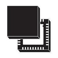
L6722TR STMicroelectronics, L6722TR Datasheet - Page 9

L6722TR
Manufacturer Part Number
L6722TR
Description
IC BUCK ADJ 2A TRPL 36VFQFPN
Manufacturer
STMicroelectronics
Type
Step-Down (Buck)r
Datasheet
1.L6722TR.pdf
(34 pages)
Specifications of L6722TR
Internal Switch(s)
No
Synchronous Rectifier
No
Number Of Outputs
3
Voltage - Output
Adj to 0.8V
Current - Output
2A
Frequency - Switching
100kHz
Voltage - Input
12V
Operating Temperature
0°C ~ 70°C
Mounting Type
Surface Mount
Package / Case
36-VFQFN, 36-VFQFPN
Power - Output
3.5W
Operating Temperature Range
- 40 C to + 125 C
Mounting Style
SMD/SMT
Lead Free Status / RoHS Status
Lead free / RoHS Compliant
Other names
497-5904-2
Available stocks
Company
Part Number
Manufacturer
Quantity
Price
L6722
Table 1.
32 to 34
27, 28
Pin#
PAD
23
24
25
26
29
30
31
35
36
Pins description (continued)
OSC / INH /
THERMAL
REF_OUT
REF_IN
SGND
ISEN3
ISEN1
Name
FBG
N.C.
N.C.
FBR
CS+
PAD
CS-
FLT
to
Three functional pin:
OSC: It allows programming the switching frequency F
channel: the equivalent switching frequency at the load side results in
being tripled.
Frequency is programmed according to the resistor connected from the
pin vs. SGND or VCC with a gain of 4kHz/µA (see relevant section for
details). Leaving the pin floating programs a switching frequency of
100kHz per phase (300kHz on the load).
INH: Forced low, the device stops operations with all mosfets OFF: all the
protections are disabled except for
device from any latching condition.
FLT: The pin is forced high (5V) to signal an OVP FAULT: to recover from
this condition, cycle VCC or the OSC pin. See
Not Internally Bonded.
REFrence INput for the regulation. Connect directly or through a resistor
to the REF_OUT pin. See
REFrence OUTput. Connect directly or through a resistor to the REF_IN
pin. See
Not Internally Bonded.
All the internal references are referred to this pin. Connect to the PCB
Signal Ground.
Remote Buffer Non Inverting Input.
Connect to the positive side of the load to perform remote sense.
See
Remote Buffer Inverting Input.
Connect to the negative side of the load to perform remote sense.
See
LS Current Sense Pins.
These pins are used for current balance phase-to-phase as well as for the
system OCP. Connect through a resistor Rg to the relative PHASEx pin.
See
Droop Current Sense non-inverting input.
Connect through R-C network to the main inductors. See
details.
Droop Current Sense inverting input.
Connect through resistor R
Section 7.1
This pin also monitor the feedback disconnection. See
details.
Thermal pad connects the Silicon substrate and makes good thermal
contact with the PCB to dissipate the power necessary to drive the
external mosfets.
Connect to the PGND plane with several VIAs to improve thermal
conductivity.
Section 12
Section 12
Section 6
Section 7.1
for details.
and
for proper layout of this connection.
for proper layout of this connection.
Section 9.6
for details.
Section 7.1
D
to the main inductors common node. See
2 Pins description and connection diagrams
for details.
Function
Preliminary over
for details.
Section 10
voltage. It resets the
SW
Section 9.4
Section 7.1
for details.
of each
for
9/34
for


