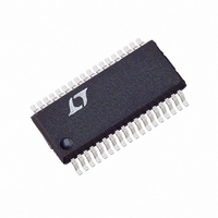
LTC3716EG Linear Technology, LTC3716EG Datasheet - Page 11

LTC3716EG
Manufacturer Part Number
LTC3716EG
Description
IC SW REG STP-DN 5BIT SYNC36SSOP
Manufacturer
Linear Technology
Type
Step-Down (Buck)r
Datasheet
1.LTC3716EG.pdf
(28 pages)
Specifications of LTC3716EG
Internal Switch(s)
No
Synchronous Rectifier
Yes
Number Of Outputs
1
Voltage - Output
0.6 ~ 1.75 V
Current - Output
35mA
Frequency - Switching
120kHz ~ 310kHz
Voltage - Input
4 ~ 36 V
Operating Temperature
-40°C ~ 85°C
Mounting Type
Surface Mount
Package / Case
36-SSOP
Lead Free Status / RoHS Status
Contains lead / RoHS non-compliant
Power - Output
-
Available stocks
Company
Part Number
Manufacturer
Quantity
Price
Company:
Part Number:
LTC3716EG
Manufacturer:
KSS
Quantity:
50 000
Part Number:
LTC3716EG
Manufacturer:
LINEAR/凌特
Quantity:
20 000
Part Number:
LTC3716EG#PBF
Manufacturer:
LINEAR/凌特
Quantity:
20 000
Company:
Part Number:
LTC3716EG#TRPBF
Manufacturer:
Linear
Quantity:
736
Part Number:
LTC3716EG#TRPBF
Manufacturer:
LT/凌特
Quantity:
20 000
Company:
Part Number:
LTC3716EG-ES
Manufacturer:
LT
Quantity:
24
Part Number:
LTC3716EGN
Manufacturer:
LT/凌特
Quantity:
20 000
OPERATIO
Frequency Synchronization
The phase-locked loop allows the internal oscillator to be
synchronized to an external source via the PLLIN pin. The
output of the phase detector at the PLLFLTR pin is also the
DC frequency control input of the oscillator that operates
over a 140kHz to 310kHz range corresponding to a DC
voltage input from 0V to 2.4V. When locked, the PLL aligns
the turn on of the top MOSFET to the rising edge of the
synchronizing signal. When PLLIN is left open, the PLLFLTR
pin goes low, forcing the oscillator to minimum frequency.
Input capacitance ESR requirements and efficiency losses
are substantially reduced because the peak current drawn
from the input capacitor is effectively divided by two and
power loss is proportional to the RMS current squared. A
two stage, single output voltage implementation can
reduce input path power loss by 75% and radically reduce
the required RMS current rating of the input capacitor(s).
INTV
Power for the top and bottom MOSFET drivers and most
of the IC circuitry is derived from INTV
EXTV
regulator supplies INTV
taken above 4.8V, the 5V regulator is turned off and an
internal switch is turned on connecting EXTV
This allows the INTV
efficiency external source such as the output of the regu-
lator itself or a secondary winding, as described in the
Applications Information section. An external Schottky
diode can be used to minimize the voltage drop from
EXTV
the specified INTV
applied to EXTV
Differential Amplifier
This amplifier provides true differential output voltage
sensing. Sensing both V
tion in high current applications and/or applications hav-
ing electrical interconnection losses. The AMPMD pin
allows selection of internal precision feedback resistors
for high common mode rejection differencing applica-
tions, or direct access to the actual amplifier inputs with-
out these internal feedback resistors for other applications.
CC
CC
CC
/EXTV
to INTV
pin is left open, an internal 5V low dropout
CC
CC
CC
Power
U
CC
for additional gate drive capability.
in applications requiring greater than
CC
current. Voltages up to 7V can be
(Refer to Functional Diagram)
power to be derived from a high
CC
OUT
power. If the EXTV
+
and V
OUT
–
benefits regula-
CC
CC
. When the
to INTV
CC
pin is
CC
.
The AMPMD pin is grounded to connect the internal pre-
cision resistors in a unity-gain differencing application or
tied to the INTV
make the amplifier inputs directly available. The amplifier
is a unity-gain stable, 2MHz gain-bandwidth, >120dB
open-loop gain design. The amplifier has an output slew
rate of 5V/ s and is capable of driving capacitive loads
with an output RMS current typically up to 25mA. The
amplifier is not capable of sinking current and therefore
must be resistively loaded to do so.
Output Overvoltage Protection
An overvoltage comparator, 0V, guards against transient
overshoots (>10%) as well as other more serious condi-
tions that may overvoltage the output. In this case, the top
MOSFET is turned off and the bottom MOSFET is turned on
until the overvoltage condition is cleared.
Power Good (PGOOD)
The PGOOD pin is connected to the drain of an internal
MOSFET. The MOSFET turns on when the output voltage
is not within 10% of its nominal output level as deter-
mined by the feedback divider. When the output is within
10 s and the PGOOD pin should be pulled up by an
external resistor to a source of up to 7V.
Short-Circuit Detection
The RUN/SS capacitor is used initially to limit the inrush
current from the input power source. Once the control-
lers have been given time, as determined by the capacitor
on the RUN/SS pin, to charge up the output capacitors
and provide full-load current, the RUN/SS capacitor is
then used as a short-circuit timeout circuit. If the output
voltage falls to less than 70% of its nominal output
voltage the RUN/SS capacitor begins discharging as-
suming that the output is in a severe overcurrent and/or
short-circuit condition. If the condition lasts for a long
enough period as determined by the size of the RUN/SS
capacitor, the controller will be shut down until the
RUN/SS pin voltage is recycled. This built-in latchoff can
be overidden by providing a current >5 A at a compli-
ance of 5V to the RUN/SS pin. This current shortens the
10% of its nominal value, the MOSFET is turned off within
CC
pin to bypass the internal resistors and
LTC3716
11


