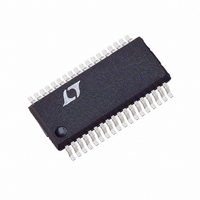
LTC3716EG Linear Technology, LTC3716EG Datasheet - Page 24

LTC3716EG
Manufacturer Part Number
LTC3716EG
Description
IC SW REG STP-DN 5BIT SYNC36SSOP
Manufacturer
Linear Technology
Type
Step-Down (Buck)r
Datasheet
1.LTC3716EG.pdf
(28 pages)
Specifications of LTC3716EG
Internal Switch(s)
No
Synchronous Rectifier
Yes
Number Of Outputs
1
Voltage - Output
0.6 ~ 1.75 V
Current - Output
35mA
Frequency - Switching
120kHz ~ 310kHz
Voltage - Input
4 ~ 36 V
Operating Temperature
-40°C ~ 85°C
Mounting Type
Surface Mount
Package / Case
36-SSOP
Lead Free Status / RoHS Status
Contains lead / RoHS non-compliant
Power - Output
-
Available stocks
Company
Part Number
Manufacturer
Quantity
Price
Company:
Part Number:
LTC3716EG
Manufacturer:
KSS
Quantity:
50 000
Part Number:
LTC3716EG
Manufacturer:
LINEAR/凌特
Quantity:
20 000
Part Number:
LTC3716EG#PBF
Manufacturer:
LINEAR/凌特
Quantity:
20 000
Company:
Part Number:
LTC3716EG#TRPBF
Manufacturer:
Linear
Quantity:
736
Part Number:
LTC3716EG#TRPBF
Manufacturer:
LT/凌特
Quantity:
20 000
Company:
Part Number:
LTC3716EG-ES
Manufacturer:
LT
Quantity:
24
Part Number:
LTC3716EGN
Manufacturer:
LT/凌特
Quantity:
20 000
APPLICATIO S I FOR ATIO
LTC3716
The worst-case power disipated by the synchronous
MOSFET under normal operating conditions at elevated
ambient temperature and estimated 50 C junction tem-
perature rise is:
A short-circuit to ground will result in a folded back current
of about:
The worst-case power disipated by the synchronous
MOSFET under short-circuit conditions at elevated ambi-
ent temperature and estimated 50 C junction temperature
rise is:
which is less than normal, full-load conditions. Inciden-
tally, since the load no longer dissipates power in the
shorted condition, total system power dissipation is de-
creased by over 99%.
The duty factor for this application is:
Using Figure 4, the RMS ripple current will be:
24
I
P
P
I
P
DF
SC
INRMS
MAIN
SYNC
SYNC
V
0 004
V
= (20A)(0.25) = 5A
25
IN
.
O
0 013
1 2
5 5
1 5
696
300
5 5
5 5
.
mV
.
.
.
.
.
W
1 2
V
V
V
V
5 5
5 5
mW
kHz
5
.
.
.
V
10
V
V
V
U
1 2
1 2
2
1
.
.
2
1 7 5 5
V
V
0 24
.
200
1
0 45
.
2 10
.
U
6 8
ns
.
.
1
0 005 110
W
RMS
A
.
V
A
H
5 5
2
2
.
2
1 48 0 013
10
V
1 48 0 013
W
.
.
A
300
6 8
C
.
.
.
A
pF
25
U
C
An input capacitor(s) with a 5A
required.
The output capacitor ripple current is calculated by using
the inductor ripple already calculated for each inductor
and multiplying by the factor obtained from Figure 3
along with the calculated duty factor. The output ripple in
continuous mode will be highest at the maximum input
voltage since the duty factor is < 50%. The maximum
output current ripple is:
PC Board Layout Checklist
When laying out the printed circuit board, the following
checklist should be used to ensure proper operation of the
LTC3716. Check the following in your layout:
1) Are the signal and power grounds separate? The signal
ground traces should return to Pin 9 first. Connect Pin 9
to Pin 28 through a wide and straight trace. Then the signal
ground joins the power ground plane beside Pin 28. It is
recommended that the Pin 28 return to the (–) plates of
C
2) Does the LTC3716 V
load? Does the LTC3716 V
return?
IN
TRACE TO INDUCTOR
V
.
OUTRIPPLE
I
I
COUT
COUTMAX
Figure 10. Proper Current Sense Connections
V
OUT
fL
2
20
PADS OF SENSE RESISTOR
300
A
SENSE
m
0 5
P P
-
.
kHz
1 2
+
OS
at
2
.
A
+
24
V
P P
1 0
SENSE
OS
pin connect to the point of
-
.
%
RMS
–
pin connect to the load
D F
–
H
ripple current rating is
40
0 5
.
mV
TRACE TO OUTPUT CAP (+)
P P
-
3716 F10


