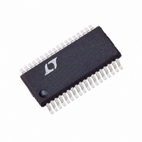
LTC3716EG Linear Technology, LTC3716EG Datasheet - Page 21

LTC3716EG
Manufacturer Part Number
LTC3716EG
Description
IC SW REG STP-DN 5BIT SYNC36SSOP
Manufacturer
Linear Technology
Type
Step-Down (Buck)r
Datasheet
1.LTC3716EG.pdf
(28 pages)
Specifications of LTC3716EG
Internal Switch(s)
No
Synchronous Rectifier
Yes
Number Of Outputs
1
Voltage - Output
0.6 ~ 1.75 V
Current - Output
35mA
Frequency - Switching
120kHz ~ 310kHz
Voltage - Input
4 ~ 36 V
Operating Temperature
-40°C ~ 85°C
Mounting Type
Surface Mount
Package / Case
36-SSOP
Lead Free Status / RoHS Status
Contains lead / RoHS non-compliant
Power - Output
-
Available stocks
Company
Part Number
Manufacturer
Quantity
Price
Company:
Part Number:
LTC3716EG
Manufacturer:
KSS
Quantity:
50 000
Part Number:
LTC3716EG
Manufacturer:
LINEAR/凌特
Quantity:
20 000
Part Number:
LTC3716EG#PBF
Manufacturer:
LINEAR/凌特
Quantity:
20 000
Company:
Part Number:
LTC3716EG#TRPBF
Manufacturer:
Linear
Quantity:
736
Part Number:
LTC3716EG#TRPBF
Manufacturer:
LT/凌特
Quantity:
20 000
Company:
Part Number:
LTC3716EG-ES
Manufacturer:
LT
Quantity:
24
Part Number:
LTC3716EGN
Manufacturer:
LT/凌特
Quantity:
20 000
APPLICATIO S I FOR ATIO
In order to prevent erratic operation if no external connec-
tions are made to the FCB pin, the FCB pin has a 0.18 A
internal current source pulling the pin high. Include this
current when choosing resistor values R5 and R6.
The following table summarizes the possible states avail-
able on the FCB pin:
Table 2
FCB Pin
0.65V < V
Feedback Resistors
>4.8V
Active Voltage Positioning
Active voltage positioning can be used to minimize peak-
to-peak output voltage excursion under worst-case tran-
sient loading conditions. The open-loop DC gain of the
control loop is reduced depending upon the maximum
load step specifications. Active voltage positioning can
easily be added to the LTC3716 by loading the I
a resistive divider having a Thevenin equivalent voltage
source equal to the midpoint operating voltage of the error
amplifier, or 1.2V (see Figure 8).
The resistive load reduces the DC loop gain while main-
taining the linear control range of the error amplifier. The
worst-case peak-to-peak output voltage deviation due to
transient loading can theoretically be reduced to half or
0V to 0.55V
Figure 8. Active Voltage Positioning Applied to the LTC3716
FCB
< 4.3V (typ)
INTV
CC
R
R
T2
T1
U
R
C
C
C
U
Condition
Forced Continuous (Current Reversal
Allowed—Burst Inhibited)
Minimum Peak Current Induces
Burst Mode Operation
No Current Reversal Allowed
Regulating a Secondary Winding
Burst Mode Operation Disabled
Constant Frequency Mode Enabled
No Current Reversal Allowed
No Minimum Peak Current
I
TH
LTC3716
W
3716 F08
TH
U
pin with
alternatively the amount of output capacitance can
be reduced for a particular application. A complete
explanation is included in Design Solutions 10 or the
LTC1736 data sheet. (See www.linear-tech.com)
Efficiency Considerations
The percent efficiency of a switching regulator is equal to
the output power divided by the input power times 100%.
It is often useful to analyze individual losses to determine
what is limiting the efficiency and which change would
produce the most improvement. Percent efficiency can be
expressed as:
where L1, L2, etc. are the individual losses as a percentage
of input power.
Although all dissipative elements in the circuit produce
losses, four main sources usually account for most of the
losses in LTC3716 circuits: 1) I
MOSFET transition losses, 3) INTV
and 4) LTC3716 V
differential amplifier output).
1) I
fuse (if used), MOSFET, inductor, current sense resistor,
and input and output capacitor ESR. In continuous mode
the average output current flows through L and R
but is “chopped” between the topside MOSFET and the
synchronous MOSFET. If the two MOSFETs have approxi-
mately the same R
MOSFET can simply be summed with the resistances of L,
R
R
total resistance is 25m . This results in losses ranging
from 2% to 8% as the output current increases from 3A to
15A per output stage for a 5V output, or a 3% to 12% loss
per output stage for a 3.3V output. Efficiency varies as the
inverse square of V
and output power level. The combined effects of increas-
ingly lower output voltages and higher currents required
by high performance digital systems is not doubling but
quadrupling the importance of loss terms in the switching
regulator system!
SENSE
DS(ON)
%Efficiency = 100% – (L1 + L2 + L3 + ...)
2
R losses are predicted from the DC resistances of the
and ESR to obtain I
= 10m , R
L
OUT
IN
= 10m , and R
DS(ON)
current (including loading on the
for the same external components
2
, then the resistance of one
R losses. For example, if each
2
R losses, 2) Topside
SENSE
CC
regulator current
= 5m , then the
LTC3716
21
SENSE
,


