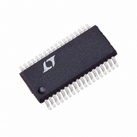
LTC3716EG Linear Technology, LTC3716EG Datasheet - Page 25

LTC3716EG
Manufacturer Part Number
LTC3716EG
Description
IC SW REG STP-DN 5BIT SYNC36SSOP
Manufacturer
Linear Technology
Type
Step-Down (Buck)r
Datasheet
1.LTC3716EG.pdf
(28 pages)
Specifications of LTC3716EG
Internal Switch(s)
No
Synchronous Rectifier
Yes
Number Of Outputs
1
Voltage - Output
0.6 ~ 1.75 V
Current - Output
35mA
Frequency - Switching
120kHz ~ 310kHz
Voltage - Input
4 ~ 36 V
Operating Temperature
-40°C ~ 85°C
Mounting Type
Surface Mount
Package / Case
36-SSOP
Lead Free Status / RoHS Status
Contains lead / RoHS non-compliant
Power - Output
-
Available stocks
Company
Part Number
Manufacturer
Quantity
Price
Company:
Part Number:
LTC3716EG
Manufacturer:
KSS
Quantity:
50 000
Part Number:
LTC3716EG
Manufacturer:
LINEAR/凌特
Quantity:
20 000
Part Number:
LTC3716EG#PBF
Manufacturer:
LINEAR/凌特
Quantity:
20 000
Company:
Part Number:
LTC3716EG#TRPBF
Manufacturer:
Linear
Quantity:
736
Part Number:
LTC3716EG#TRPBF
Manufacturer:
LT/凌特
Quantity:
20 000
Company:
Part Number:
LTC3716EG-ES
Manufacturer:
LT
Quantity:
24
Part Number:
LTC3716EGN
Manufacturer:
LT/凌特
Quantity:
20 000
APPLICATIO S I FOR ATIO
3) Are the SENSE
minimum PC trace spacing? The filter capacitors between
SENSE
possible to the LTC3716. Ensure accurate current sensing
with Kelvin connections at the current sense resistor. See
Figure 10.
4) Does the (+) plate of C
topside MOSFETs as closely as possible? This capacitor
provides the AC current to the MOSFETs. Keep the input
current path formed by the input capacitor, top and bottom
MOSFETs, and the Schottky diode on the same side of the
PC board in a tight loop to minimize conducted and
radiated EMI.
5) Is the INTV
nected closely between INTV
capacitor carries the MOSFET driver peak currents. A
small value is recommended to allow placement immedi-
ately adjacent to the IC.
+
and SENSE
R
IN
CC
V
IN
–
1 F ceramic decoupling capacitor con-
C
and SENSE
IN
BOLD LINES INDICATE
HIGH, SWITCHING
CURRENT LINES.
KEEP LINES TO A
MINIMUM LENGTH.
U
+
–
Figure 11. Instantaneous Current Path Flow in a Multiple Phase Switching Regulator
pin pairs should be as close as
IN
U
connect to the drains of the
CC
+
leads routed together with
and the PGND pin? This
W
SW1
SW2
U
D1
D2
L1
L2
6) Keep the switching nodes, SW1 (SW2), away from
sensitive small-signal nodes. Ideally the switch nodes
should be placed at the furthest point from the
LTC3716.
7) Use a low impedance source such as a logic gate to drive
the PLLIN pin and keep the lead as short as possible.
The diagram in Figure 11 illustrates all branch currents in
a 2-phase switching regulator. It becomes very clear after
studying the current waveforms why it is critical to keep
the high-switching-current paths to a small physical size.
High electric and magnetic fields will radiate from these
“loops” just as radio stations transmit signals. The output
capacitor ground should return to the negative terminal of
the input capacitor and not share a common ground path
with any switched current paths. The left half of the circuit
gives rise to the “noise” generated by a switching regula-
tor. The ground terminations of the sychronous MOSFETs
and Schottky diodes should return to the negative plate(s)
R
R
SENSE1
SENSE2
3716 F11
+
C
V
OUT
OUT
LTC3716
R
L
25


