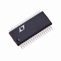
LTC3716EG Linear Technology, LTC3716EG Datasheet - Page 26

LTC3716EG
Manufacturer Part Number
LTC3716EG
Description
IC SW REG STP-DN 5BIT SYNC36SSOP
Manufacturer
Linear Technology
Type
Step-Down (Buck)r
Datasheet
1.LTC3716EG.pdf
(28 pages)
Specifications of LTC3716EG
Internal Switch(s)
No
Synchronous Rectifier
Yes
Number Of Outputs
1
Voltage - Output
0.6 ~ 1.75 V
Current - Output
35mA
Frequency - Switching
120kHz ~ 310kHz
Voltage - Input
4 ~ 36 V
Operating Temperature
-40°C ~ 85°C
Mounting Type
Surface Mount
Package / Case
36-SSOP
Lead Free Status / RoHS Status
Contains lead / RoHS non-compliant
Power - Output
-
Available stocks
Company
Part Number
Manufacturer
Quantity
Price
Company:
Part Number:
LTC3716EG
Manufacturer:
KSS
Quantity:
50 000
Part Number:
LTC3716EG
Manufacturer:
LINEAR/凌特
Quantity:
20 000
Part Number:
LTC3716EG#PBF
Manufacturer:
LINEAR/凌特
Quantity:
20 000
Company:
Part Number:
LTC3716EG#TRPBF
Manufacturer:
Linear
Quantity:
736
Part Number:
LTC3716EG#TRPBF
Manufacturer:
LT/凌特
Quantity:
20 000
Company:
Part Number:
LTC3716EG-ES
Manufacturer:
LT
Quantity:
24
Part Number:
LTC3716EGN
Manufacturer:
LT/凌特
Quantity:
20 000
LTC3716
APPLICATIO S I FOR ATIO
of the input capacitor(s) with a short isolated PC trace
since very high switched currents are present. A separate
isolated path from the negative plate(s) of the input
capacitor(s) should be used to tie in the IC power ground
pin (PGND) and the signal ground pin (SGND). This
technique keeps inherent signals generated by high cur-
rent pulses from taking alternate current paths that have
finite impedances during the total period of the switching
regulator. External OPTI-LOOP compensation allows over-
compensation for PC layouts which are not optimized but
this is not the recommended design procedure.
Simplified Visual Explanation of How a 2-Phase
Controller Reduces Both Input and Output RMS Ripple
Current
A multiphase power supply significantly reduces the
amount of ripple current in both the input and output
capacitors. The RMS input ripple current is divided by, and
the effective ripple frequency is multiplied up by the
number of phases used (assuming that the input voltage
is greater than the number of phases used times the output
voltage). The output ripple amplitude is also reduced by,
and the effective ripple frequency is increased by the
number of phases used. Figure 12 graphically illustrates
the principle.
The worst-case RMS ripple current for a single stage
design peaks at an input voltage of twice the output
26
SW V
I
COUT
I
CIN
Figure 12. Single and 2-Phase Current Waveforms
SINGLE PHASE
U
U
SW1 V
SW2 V
I
COUT
I
CIN
I
I
L1
L2
W
DUAL PHASE
U
RIPPLE
3216 F12
voltage. The worst-case RMS ripple current for a two stage
design results in peak outputs of 1/4 and 3/4 of input
voltage. When the RMS current is calculated, higher
effective duty factor results and the peak current levels are
divided as long as the currents in each stage are balanced.
Refer to Application Note 19 for a detailed description of
how to calculate RMS current for the single stage switch-
ing regulator. Figures 3 and 4 illustrate how the input and
output currents are reduced by using an additional phase.
The input current peaks drop in half and the frequency is
doubled for this 2-phase converter. The input capacity
requirement is thus reduced theoretically by a factor of
four! Ceramic input capacitors with their unbeatably low
ESR characteristics can be used.
Figure 4 illustrates the RMS input current drawn from the
input capacitance vs the duty cycle as determined by the
ratio of input and output voltage. The peak input RMS
current level of the single phase system is reduced by 50%
in a 2-phase solution due to the current splitting between
the two stages.
An interesting result of the 2-phase solution is that the V
which produces worst-case ripple current for the input
capacitor, V
duces zero input current ripple in the 2-phase design.
The output ripple current is reduced significantly when
compared to the single phase solution using the same
inductance value because the V
term from the stage that has its bottom MOSFET on
subtracts current from the (V
resulting from the stage which has its top MOSFET on. The
output ripple current is:
where D is duty factor.
The input and output ripple frequency is increased by the
number of stages used, reducing the output capacity
requirements. When V
as illustrated in Figures 3 and 4, very low input and output
ripple currents result.
I
RIPPLE
OUT
2
= V
V
fL
OUT
IN
/2, in the single phase design pro-
IN
1 2
is approximately equal to 2(V
1 2
D
IN
D
– V
1
OUT
OUT
1
D
/L discharge current
)/L charging current
OUT
IN
)


