L6727 STMicroelectronics, L6727 Datasheet - Page 15

L6727
Manufacturer Part Number
L6727
Description
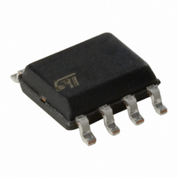
IC PWM CTLR SGL PHASE SO-8
Manufacturer
STMicroelectronics
Type
Step-Down (Buck)r
Datasheet
1.L6727TR.pdf
(34 pages)
Specifications of L6727
Internal Switch(s)
No
Synchronous Rectifier
No
Number Of Outputs
1
Voltage - Output
Adj to 0.8V
Frequency - Switching
300kHz
Voltage - Input
1.5 ~ 12 V
Operating Temperature
-20°C ~ 85°C
Mounting Type
Surface Mount
Package / Case
8-SOIC (3.9mm Width)
Output Current
1.5 A
Input Voltage
- 0.3 V to + 15 V
Switching Frequency
300 KHz
Operating Temperature Range
- 40 C to + 150 C
Mounting Style
SMD/SMT
Duty Cycle (max)
80 %
For Use With
497-8266 - BOARD EVAL BASED ON L6727497-6258 - BOARD EVAL 1PH STPDWN CONV L6727
Lead Free Status / RoHS Status
Lead free / RoHS Compliant
Current - Output
-
Power - Output
-
Lead Free Status / Rohs Status
Lead free / RoHS Compliant
Available stocks
Company
Part Number
Manufacturer
Quantity
Price
Part Number:
L6727
Manufacturer:
ST
Quantity:
20 000
Part Number:
L6727TR
Manufacturer:
ST
Quantity:
20 000
L6727
9
9.1
9.2
Application details
Output voltage selection
L6727 is capable to precisely regulate an output voltage as low as 0.8 V. In fact, the device
comes with a fixed 0.8 V internal reference that guarantees the output regulated voltage to
be within ±1 % tolerance over line and temperature variations between 0 °C and +70 °C
(excluding output resistor divider tolerance, when present).
Output voltage higher than 0.8 V can be easily achieved by adding a resistor R
FB pin and ground. Referring to
where V
Compensation network
The control loop showed in
voltage mode type. The output voltage is regulated to the internal reference (when present,
offset resistor between FB node and GND can be neglected in control loop calculation).
Error Amplifier output is compared to oscillator saw-tooth waveform to provide PWM signal
to the driver section. PWM signal is then transferred to the switching node with V
amplitude. This waveform is filtered by the output filter.
The converter transfer function is the small signal transfer function between the output of the
EA and V
resonance and a zero at F
modulator is simply the input voltage V
ΔV
The compensation network closes the loop joining V
function ideally equal to -Z
Figure 6.
OSC
.
REF
OUT
is 0.8V.
PWM control loop
. This function has a double pole at frequency F
ΔV
OSC
ESR
F
OSC
/Z
Figure 6
V
FB
Doc ID 12933 Rev 4
OUT
depending on the output capacitor ESR. The DC Gain of the
COMPARATOR
AMPLIFIER
Figure
.
ERROR
C
F
_
+
PWM
C
P
is a voltage mode control loop. The error amplifier is a
=
R
+
_
IN
F
1, the steady state DC output voltage will be:
V
divided by the peak-to-peak oscillator voltage
REF
V
REF
Z
F
⋅
R
C
⎛
⎝
FB
S
1
V
IN
+
R
OUT
S
Z
---------- -
R
R
FB
L
OS
FB
and EA output with transfer
⎞
⎠
LC
R
C
ESR
OUT
depending on the L-C
V
Application details
OUT
OS
IN
between
OUT
15/34


