L6727 STMicroelectronics, L6727 Datasheet - Page 21

L6727
Manufacturer Part Number
L6727
Description
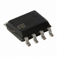
IC PWM CTLR SGL PHASE SO-8
Manufacturer
STMicroelectronics
Type
Step-Down (Buck)r
Datasheet
1.L6727TR.pdf
(34 pages)
Specifications of L6727
Internal Switch(s)
No
Synchronous Rectifier
No
Number Of Outputs
1
Voltage - Output
Adj to 0.8V
Frequency - Switching
300kHz
Voltage - Input
1.5 ~ 12 V
Operating Temperature
-20°C ~ 85°C
Mounting Type
Surface Mount
Package / Case
8-SOIC (3.9mm Width)
Output Current
1.5 A
Input Voltage
- 0.3 V to + 15 V
Switching Frequency
300 KHz
Operating Temperature Range
- 40 C to + 150 C
Mounting Style
SMD/SMT
Duty Cycle (max)
80 %
For Use With
497-8266 - BOARD EVAL BASED ON L6727497-6258 - BOARD EVAL 1PH STPDWN CONV L6727
Lead Free Status / RoHS Status
Lead free / RoHS Compliant
Current - Output
-
Power - Output
-
Lead Free Status / Rohs Status
Lead free / RoHS Compliant
Available stocks
Company
Part Number
Manufacturer
Quantity
Price
Part Number:
L6727
Manufacturer:
ST
Quantity:
20 000
Part Number:
L6727TR
Manufacturer:
ST
Quantity:
20 000
L6727
10.2
10.3
Output capacitors
Output capacitors choice depends on the application constraints in point of output voltage
ripple and output voltage deviation during a load transient.
During steady-state conditions, the output voltage ripple is influenced by ESR and
capacitance of the output capacitors as follows:
Where ΔI
will be lower than the sum of their moduli. Even ESL and board parasitic inductance can
contribute significantly to output ripple.
During a load variation, the output capacitors supply to the load the additional current or
absorb the current in excess delivered by the inductor until converter reaction is completed.
In fact, even if the controller react immediately to the load transient saturating the duty cycle
to 80 % or 0 %, the current slew rate is limited by the inductance. At first approximation,
output voltage drop, based on ESR and capacitor charge/discharge and considering an
ideal load-step, can be estimated as follows:
Where ΔV
the load appliance or V
MLCC capacitors typically have low ESR to minimize the ripple but also have low
capacitance that do not minimize the capacitive voltage deviation during load transient. On
the contrary, electrolytic capacitors usually have higher capacitance to minimize capacitive
voltage deviation during load transient, but also higher ESR value resulting in higher ripple
voltage and resistive voltage drop. For these reasons, a mix between electrolytic and MLCC
capacitor is usually suggested to minimize ripple as well as reducing voltage deviation in
dynamic conditions.
Input capacitors
The input capacitor bank is designed mainly to stand input rms current, which depends on
output current (I
The equation reaches its maximum value, I
capacitor ESR:
ΔV
ΔV
ΔV
I
ΔV
P
rms
=
OUT_ESR
OUT_C
OUT_ESR
OUT_C
=
ESR I
I
OUT
L
=
=
L
⋅
is the inductor current ripple. These contribution are not in phase, so total ripple
=
ΔI
=
is the voltage applied to the inductor during the transient (
⋅
rms
------------------------------------- -
2 C
L
⋅
ΔI
ΔI
L ΔI
D
2
⋅
⋅
L
OUT
OUT
-------------------------------------- -
8 C
⋅
OUT
⋅
(
⋅
1 D
ESR
OUT
–
⋅
) and duty-cycle (D) for the regulation as follows:
OUT
⋅
ESR
ΔV
1
2
)
OUT
L
⋅
F
SW
for the load removal).
Doc ID 12933 Rev 4
OUT
/2, when D = 0.5. Losses depend on input
Application information
D
MAX
⋅
V
IN
–
V
OUT
21/34
for


