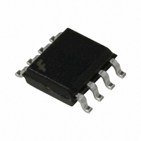
FAN5037M Fairchild Semiconductor, FAN5037M Datasheet - Page 2

FAN5037M
Manufacturer Part Number
FAN5037M
Description
IC CTRLR DC/DC SW HP ADJ 8SOIC
Manufacturer
Fairchild Semiconductor
Type
Step-Down (Buck)r
Datasheet
1.FAN5037MX.pdf
(11 pages)
Specifications of FAN5037M
Internal Switch(s)
No
Synchronous Rectifier
No
Number Of Outputs
1
Voltage - Output
1.2 ~ 3.6 V
Current - Output
13A
Voltage - Input
5V
Operating Temperature
0°C ~ 70°C
Mounting Type
Surface Mount
Package / Case
8-SOIC (3.9mm Width)
Output Voltage
1.2 V to 3.6 V
Output Current
13 A
Input Voltage
9.5 V to 12.6 V
Operating Temperature Range
0 C to + 70 C
Mounting Style
SMD/SMT
Duty Cycle (max)
85 %
Lead Free Status / RoHS Status
Lead free / RoHS Compliant
Power - Output
-
Frequency - Switching
-
Lead Free Status / Rohs Status
Lead free / RoHS Compliant
Other names
FAN5037M_NL
FAN5037M_NL
FAN5037M_NL
Available stocks
Company
Part Number
Manufacturer
Quantity
Price
Company:
Part Number:
FAN5037M
Manufacturer:
Fairchild Semiconductor
Quantity:
135
Part Number:
FAN5037M
Manufacturer:
FAIRCHILD/仙童
Quantity:
20 000
FAN5037
Pin Assignments
Pin Descriptions
Absolute Maximum Ratings
Note:
1. Functional operation under any of these conditions is not implied. Performance is guaranteed only if Operating Conditions
Operating Conditions
2
Supply Voltages, VCCA
Supply Voltages, VCCP
Junction Temperature, T
Storage Temperature, T
Lead Soldering Temperature, 10 seconds
Thermal Resistance Junction-to-Ambient,
Parameter
Switching Regulator Supply, VCCA
Ambient Operating Temperature, T
Gate Drive Supply, VCCP
GNDP
VCCA
VCCP
Name
CEXT
IFBH
IFBL
DRV
VFB
are not exceeded.
Pin
Number
Pin
1
2
3
4
5
6
7
8
Pin Function Description
External capacitor. A 180pF capacitor is connected to this pin as part of the constant
on-time pulse width circuit. Careful layout of this pin is critical to system performance.
See Applications Information for details.
Analog V
system 5V supply and decouple to ground with 0.1µF ceramic capacitor.
High side current feedback. Pins 3 and 4 are used as the inputs for the current feedback
control loop and as the short circuit current sense points. Careful layout of the traces from
these pins to the current sense resistor is critical for optimal performance of the short circuit
protection scheme. See Applications Information for details.
Low side current feedback. See Applications Information for details.
Voltage feedback. Using two external resistors, this pin sets the output voltage level for the
switching regulator.
Power Ground. Connect to a low impedance ground. See Application Information for
details.
MOSFET driver output. Connect this pin to the gate of the N-channel MOSFET Q1 as
shown in Figure 12. The trace from this pin to the MOSFET gate should be kept as short as
possible (less than 0.5"). See Applications Information for details.
Power V
filter shown in Figure 12. See Applications Information for details.
S
J
cc
cc
. Power supply for DRV output driver. Connect to system 12V supply with R-C
. Power supply for regulator control circuitry and voltage reference. Connect to
A
VCCA
CEXT
IFBH
IFBL
JA
Conditions
1
2
3
4
FAN5037
8
7
6
5
VCCP
DRV
GNDP
VFB
Min.
4.75
9.5
0
Typ.
12
-65 to +150°C
5
163°C/W
PRODUCT SPECIFICATION
+150°C
300°C
13V
7V
Max.
5.25
12.6
REV. 1.0.3 9/26/01
70
Units
°C
V
V


