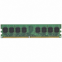
HYS64T128020HU-3S-B Qimonda, HYS64T128020HU-3S-B Datasheet - Page 19

HYS64T128020HU-3S-B
Manufacturer Part Number
HYS64T128020HU-3S-B
Description
MODULE DDR2 1GB 240-DIMM
Manufacturer
Qimonda
Datasheet
1.HYS64T64000HU-3S-B.pdf
(87 pages)
Specifications of HYS64T128020HU-3S-B
Memory Type
DDR2 SDRAM
Memory Size
1GB
Speed
333MHz
Package / Case
240-DIMM
Lead Free Status / RoHS Status
Lead free / RoHS Compliant
Other names
675-1024
1) Timings are guaranteed with CK/CK differential Slew Rate of 2.0 V/ns. For DQS signals timings are guaranteed with a differential Slew
2) The CK/CK input reference level (for timing reference to CK/CK) is the point at which CK and CK cross. The DQS / DQS, RDQS / RDQS,
3) Inputs are not recognized as valid until
4) The output timing reference voltage level is
5)
Rev. 1.3, 2006-12
03292006-6GMD-RSFT
Speed Grade
QAG Sort Name
CAS-RCD-RP latencies
Parameter
Row Active Time
Row Cycle Time
RAS-CAS-Delay
Row Precharge Time
Speed Grade
QAG Sort Name
CAS-RCD-RP latencies
Parameter
Clock Frequency
Row Active Time
Row Cycle Time
RAS-CAS-Delay
Row Precharge Time
Rate of 2.0 V/ns in differential strobe mode and a Slew Rate of 1 V/ns in single ended mode. Timings are further guaranteed for normal
OCD drive strength (EMRS(1) A1 = 0) .
input reference level is the crosspoint when in differential strobe mode
t
Rate of 2.0 V/ns in differential strobe mode and a Slew Rate of 1 V/ns in single ended mode.Timings are further guaranteed for normal
OCD drive strength (EMRS(1) A1 = 0)
input reference level is the crosspoint when in differential strobe mode.
t
RAS.MAX
RAS.MAX
is calculated from the maximum amount of time a DDR2 device can operate without a refresh command which is equal to 9 x
is calculated from the maximum amount of time a DDR2 device can operate without a refresh command which is equal to 9 x
@ CL = 3
@ CL = 4
@ CL = 5
V
V
REF
REF
Symbol
t
t
t
t
V
V
RAS
RC
RCD
RP
stabilizes. During the period before
stabilizes. During the period before
TT
TT
.
.
Symbol
t
t
t
t
t
t
t
CK
CK
CK
RAS
RC
RCD
RP
DDR2–667C
–3
4–4–4
Min.
45
57
12
12
19
Speed Grade Definition Speed Bins for DDR2–533C
HYS[64/72]T[32/64/128]xx0HU-[25F/2.5/3/3S/3.7/5]-B
Max.
70000
—
—
—
DDR2–533C
–3.7
4–4–4
Min.
5
3.75
3.75
45
60
15
15
V
V
REF
REF
DDR2–667D
–3S
5–5–5
Min.
45
60
15
15
stabilizes, CKE = 0.2 x
stabilizes, CKE = 0.2 x
Max.
8
8
8
70000
—
—
—
Unbuffered DDR2 SDRAM Module
Max.
70000
—
—
—
Unit
t
—
ns
ns
ns
ns
ns
ns
ns
CK
V
V
DDQ
DDQ
Unit
t
—
ns
ns
ns
ns
CK
Internet Data Sheet
is recognized as low.
is recognized as low.
TABLE 14
Note
1)2)3)4)
1)2)3)4)
1)2)3)4)
1)2)3)4)5)
1)2)3)4)
1)2)3)4)
1)2)3)4)
Note
1)2)3)4)5)
1)2)3)4)
1)2)3)4)
1)2)3)4)
t
t
REFI
REFI
.
.


