MA180023 Microchip Technology, MA180023 Datasheet - Page 207
MA180023
Manufacturer Part Number
MA180023
Description
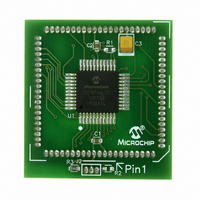
MODULE PLUG-IN PIC18F46J11 PIM
Manufacturer
Microchip Technology
Series
PIC®r
Datasheet
1.MA180023.pdf
(528 pages)
Specifications of MA180023
Accessory Type
Plug-In Module (PIM) - PIC18F46J11
Tool / Board Applications
General Purpose MCU, MPU, DSP, DSC
Mcu Supported Families
PIC18
Supported Devices
Stand-alone Or W/ HPC(DM183022) Or PIC18(DM183032)
Silicon Manufacturer
Microchip
Core Architecture
PIC
Core Sub-architecture
PIC18
Silicon Core Number
PIC18F
Silicon Family Name
PIC18FxxJxx
Lead Free Status / RoHS Status
Lead free / RoHS Compliant
For Use With/related Products
HPC Explorer Board (DM183022) or PIC18 Explorer Board (DM183032)
For Use With
DM183032 - BOARD EXPLORER PICDEM PIC18DM183022 - BOARD DEMO PIC18FXX22 64/80TQFP
Lead Free Status / RoHS Status
Lead free / RoHS Compliant
Available stocks
Company
Part Number
Manufacturer
Quantity
Price
Company:

Part Number:
MA180023
Manufacturer:
Microchip Technology
Quantity:
135


13.0
The Timer2 module incorporates the following features:
• 8-bit Timer and Period registers (TMR2 and PR2,
• Readable and writable (both registers)
• Software programmable prescaler
• Software programmable postscaler
• Interrupt on TMR2 to PR2 match
• Optional use as the shift clock for the
The module is controlled through the T2CON register
(Register 13-1) which enables or disables the timer and
configures the prescaler and postscaler. Timer2 can be
shut off by clearing control bit, TMR2ON (T2CON<2>),
to minimize power consumption.
A simplified block diagram of the module is shown in
Figure 13-1.
REGISTER 13-1:
© 2009 Microchip Technology Inc.
bit 7
Legend:
R = Readable bit
-n = Value at POR
bit 7
bit 6-3
bit 2
bit 1-0
respectively)
(1:1, 1:4 and 1:16)
(1:1 through 1:16)
MSSP modules
U-0
—
TIMER2 MODULE
Unimplemented: Read as ‘0’
T2OUTPS<3:0>: Timer2 Output Postscale Select bits
0000 = 1:1 Postscale
0001 = 1:2 Postscale
•
•
•
1111 = 1:16 Postscale
TMR2ON: Timer2 On bit
1 = Timer2 is on
0 = Timer2 is off
T2CKPS<1:0>: Timer2 Clock Prescale Select bits
00 = Prescaler is 1
01 = Prescaler is 4
1x = Prescaler is 16
T2OUTPS3
R/W-0
T2CON: TIMER2 CONTROL REGISTER (ACCESS FCAh)
W = Writable bit
‘1’ = Bit is set
T2OUTPS2
R/W-0
T2OUTPS1
R/W-0
U = Unimplemented bit, read as ‘0’
‘0’ = Bit is cleared
T2OUTPS0
PIC18F46J11 FAMILY
R/W-0
13.1
In normal operation, TMR2 is incremented from 00h on
each clock (F
clock input gives direct input, divide-by-4 and
divide-by-16 prescale options. These are selected by
the
(T2CON<1:0>). The value of TMR2 is compared to that
of the Period register, PR2, on each clock cycle. When
the two values match, the comparator generates a
match signal as the timer output. This signal also resets
the value of TMR2 to 00h on the next cycle and drives
the
“Timer2 Interrupt”).
The TMR2 and PR2 registers are both directly readable
and writable. The TMR2 register is cleared on any
device Reset, while the PR2 register initializes at FFh.
Both the prescaler and postscaler counters are cleared
on the following events:
• a write to the TMR2 register
• a write to the T2CON register
• any device Reset (Power-on Reset (POR), MCLR
TMR2 is not cleared when T2CON is written.
Reset, Watchdog Timer Reset (WDTR) or
Brown-out Reset (BOR))
output
prescaler
Timer2 Operation
TMR2ON
OSC
counter/postscaler
R/W-0
/4). A 4-bit counter/prescaler on the
control
x = Bit is unknown
T2CKPS1
R/W-0
bits,
(see
DS39932C-page 207
T2CKPS<1:0>
Section 13.2
T2CKPS0
R/W-0
bit 0
Related parts for MA180023
Image
Part Number
Description
Manufacturer
Datasheet
Request
R

Part Number:
Description:
Manufacturer:
Microchip Technology Inc.
Datasheet:
Part Number:
Description:
Manufacturer:
Microchip Technology Inc.
Datasheet:
Part Number:
Description:
Manufacturer:
Microchip Technology Inc.
Datasheet:
Part Number:
Description:
Manufacturer:
Microchip Technology Inc.
Datasheet:
Part Number:
Description:
Manufacturer:
Microchip Technology Inc.
Datasheet:
Part Number:
Description:
Manufacturer:
Microchip Technology Inc.
Datasheet:
Part Number:
Description:
Manufacturer:
Microchip Technology Inc.
Datasheet:
Part Number:
Description:
Manufacturer:
Microchip Technology Inc.
Datasheet: