MA180023 Microchip Technology, MA180023 Datasheet - Page 40
MA180023
Manufacturer Part Number
MA180023
Description
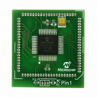
MODULE PLUG-IN PIC18F46J11 PIM
Manufacturer
Microchip Technology
Series
PIC®r
Datasheet
1.MA180023.pdf
(528 pages)
Specifications of MA180023
Accessory Type
Plug-In Module (PIM) - PIC18F46J11
Tool / Board Applications
General Purpose MCU, MPU, DSP, DSC
Mcu Supported Families
PIC18
Supported Devices
Stand-alone Or W/ HPC(DM183022) Or PIC18(DM183032)
Silicon Manufacturer
Microchip
Core Architecture
PIC
Core Sub-architecture
PIC18
Silicon Core Number
PIC18F
Silicon Family Name
PIC18FxxJxx
Lead Free Status / RoHS Status
Lead free / RoHS Compliant
For Use With/related Products
HPC Explorer Board (DM183022) or PIC18 Explorer Board (DM183032)
For Use With
DM183032 - BOARD EXPLORER PICDEM PIC18DM183022 - BOARD DEMO PIC18FXX22 64/80TQFP
Lead Free Status / RoHS Status
Lead free / RoHS Compliant
Available stocks
Company
Part Number
Manufacturer
Quantity
Price
Company:

Part Number:
MA180023
Manufacturer:
Microchip Technology
Quantity:
135


PIC18F46J11 FAMILY
2.5
When the PRI_IDLE mode is selected, the designated
primary
interruption. In secondary clock modes (SEC_RUN
and SEC_IDLE), the Timer1 oscillator is operating and
providing the device clock. The Timer1 oscillator may
also run in all power-managed modes if required to
clock Timer1 or Timer3.
In internal oscillator modes (RC_RUN and RC_IDLE),
the internal oscillator block provides the device clock
source. The 31 kHz INTRC output can be used directly
to provide the clock and may be enabled to support
various
power-managed mode (see Section 25.2 “Watchdog
Timer (WDT)”, Section 25.4 “Two-Speed Start-up”
and Section 25.5 “Fail-Safe Clock Monitor” for more
information on WDT, FSCM and Two-Speed Start-up).
The INTOSC output at 8 MHz may be used directly to
clock the device or may be divided down by the
postscaler. The INTOSC output is disabled if the clock
is provided directly from the INTRC output.
If Sleep mode is selected, all clock sources, which are
no longer required, are stopped. Since all the transistor
switching currents have been stopped, Sleep mode
achieves the lowest current consumption of the device
(only leakage currents) outside of Deep Sleep mode.
Enabling any on-chip feature that will operate during
Sleep mode increases the current consumed during
Sleep mode. The INTRC is required to support WDT
operation. The Timer1 oscillator may be operating to
support an RTC. Other features may be operating that
do not require a device clock source (i.e., MSSP slave,
PMP, INTx pins, etc.). Peripherals that may add
significant
Section 28.2 “DC Characteristics: Power-Down and
Supply Current PIC18F46J50 Family (Industrial)”.
DS39932C-page 40
Effects of Power-Managed Modes
on Various Clock Sources
special
oscillator
current
features
continues
consumption
regardless
to
are
run
listed
of
without
the
in
2.6
Power-up delays are controlled by two timers so that no
external Reset circuitry is required for most applica-
tions. The delays ensure that the device is kept in
Reset until the device power supply is stable under
normal circumstances and the primary clock is operat-
ing and stable. For additional information on power-up
delays, see Section 4.6 “Power-up Timer (PWRT)”.
The first timer is the Power-up Timer (PWRT), which
provides a fixed delay on power-up (parameter 33,
Table 28-13).
The second timer is the Oscillator Start-up Timer
(OST), intended to keep the chip in Reset until the
crystal oscillator is stable (HS mode). The OST does
this by counting 1024 oscillator cycles before allowing
the oscillator to clock the device.
There is a delay of interval, T
Table 28-13), following POR, while the controller
becomes ready to execute instructions. This delay runs
concurrently with any other delays. This may be the only
delay that occurs when any of the internal oscillator or
EC modes are used as the primary clock source.
Power-up Delays
© 2009 Microchip Technology Inc.
CSD
(parameter 38,
Related parts for MA180023
Image
Part Number
Description
Manufacturer
Datasheet
Request
R

Part Number:
Description:
Manufacturer:
Microchip Technology Inc.
Datasheet:
Part Number:
Description:
Manufacturer:
Microchip Technology Inc.
Datasheet:
Part Number:
Description:
Manufacturer:
Microchip Technology Inc.
Datasheet:
Part Number:
Description:
Manufacturer:
Microchip Technology Inc.
Datasheet:
Part Number:
Description:
Manufacturer:
Microchip Technology Inc.
Datasheet:
Part Number:
Description:
Manufacturer:
Microchip Technology Inc.
Datasheet:
Part Number:
Description:
Manufacturer:
Microchip Technology Inc.
Datasheet:
Part Number:
Description:
Manufacturer:
Microchip Technology Inc.
Datasheet: