MA180023 Microchip Technology, MA180023 Datasheet - Page 209
MA180023
Manufacturer Part Number
MA180023
Description
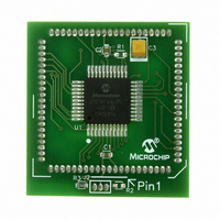
MODULE PLUG-IN PIC18F46J11 PIM
Manufacturer
Microchip Technology
Series
PIC®r
Datasheet
1.MA180023.pdf
(528 pages)
Specifications of MA180023
Accessory Type
Plug-In Module (PIM) - PIC18F46J11
Tool / Board Applications
General Purpose MCU, MPU, DSP, DSC
Mcu Supported Families
PIC18
Supported Devices
Stand-alone Or W/ HPC(DM183022) Or PIC18(DM183032)
Silicon Manufacturer
Microchip
Core Architecture
PIC
Core Sub-architecture
PIC18
Silicon Core Number
PIC18F
Silicon Family Name
PIC18FxxJxx
Lead Free Status / RoHS Status
Lead free / RoHS Compliant
For Use With/related Products
HPC Explorer Board (DM183022) or PIC18 Explorer Board (DM183032)
For Use With
DM183032 - BOARD EXPLORER PICDEM PIC18DM183022 - BOARD DEMO PIC18FXX22 64/80TQFP
Lead Free Status / RoHS Status
Lead free / RoHS Compliant
Available stocks
Company
Part Number
Manufacturer
Quantity
Price
Company:

Part Number:
MA180023
Manufacturer:
Microchip Technology
Quantity:
135


14.0
The Timer3 timer/counter module incorporates these
features:
• Software selectable operation as a 16-bit timer or
• Readable and writable 8-bit registers (TMR3H
• Selectable clock source (internal or external) with
• Interrupt-on-overflow
• Module Reset on ECCP Special Event Trigger
REGISTER 14-1:
© 2009 Microchip Technology Inc.
bit 7
Legend:
R = Readable bit
-n = Value at POR
bit 7-6
bit 5-4
bit 3
bit 2
bit 1
bit 0
Note 1:
TMR3CS1
counter
and TMR3L)
device clock or Timer1 oscillator internal options
R/W-0
TIMER3 MODULE
The F
features.
TMR3CS<1:0>: Timer3 Clock Source Select bits
10 = Timer3 clock source is
01 = Timer3 clock source is the system clock (F
00 = Timer3 clock source is the instruction clock (F
T3CKPS<1:0>: Timer3 Input Clock Prescale Select bits
11 = 1:8 Prescale value
10 = 1:4 Prescale value
01 = 1:2 Prescale value
00 = 1:1 Prescale value
Reserved: Program as ‘0’
T3SYNC: Timer3 External Clock Input Synchronization Control bit
When TMR3CS<1:0> = 10:
1 = Do not synchronize external clock input
0 = Synchronize external clock input
When TMR3CS<1:0> = 0x:
This bit is ignored; Timer3 uses the internal clock.
RD16: 16-Bit Read/Write Mode Enable bit
1 = Enables register read/write of Timer3 in one 16-bit operation
0 = Enables register read/write of Timer3 in two 8-bit operations
TMR3ON: Timer3 On bit
1 = Enables Timer3
0 = Stops Timer3
TMR3CS0
OSC
R/W-0
clock source should not be selected if the timer will be used with the ECCP capture/compare
T3CON: TIMER3 CONTROL REGISTER (ACCESS F79h)
W = Writable bit
‘1’ = Bit is set
T3CKPS1
R/W-0
th
e T3CKI input pin (assigned in the PPS module)
T3CKPS0
R/W-0
U = Unimplemented bit, read as ‘0’
‘0’ = Bit is cleared
PIC18F46J11 FAMILY
A simplified block diagram of the Timer3 module is
shown in Figure 14-1.
The Timer3 module is controlled through the T3CON
register (Register 14-1). It also selects the clock source
options for the ECCP modules; see Section 17.1.1
“ECCP Module and Timer Resources” for more
information.
The F
not be used with the ECCP capture/compare features.
If the timer will be used with the capture or compare
features, always select one of the other timer clocking
options.
OSC
U-0
—
OSC
)
(1)
OSC
/4)
clock source (TMR3CS<1:0> = 01) should
T3SYNC
R/W-0
x = Bit is unknown
R/W-0
RD16
DS39932C-page 209
TMR3ON
R/W-0
bit 0
Related parts for MA180023
Image
Part Number
Description
Manufacturer
Datasheet
Request
R

Part Number:
Description:
Manufacturer:
Microchip Technology Inc.
Datasheet:
Part Number:
Description:
Manufacturer:
Microchip Technology Inc.
Datasheet:
Part Number:
Description:
Manufacturer:
Microchip Technology Inc.
Datasheet:
Part Number:
Description:
Manufacturer:
Microchip Technology Inc.
Datasheet:
Part Number:
Description:
Manufacturer:
Microchip Technology Inc.
Datasheet:
Part Number:
Description:
Manufacturer:
Microchip Technology Inc.
Datasheet:
Part Number:
Description:
Manufacturer:
Microchip Technology Inc.
Datasheet:
Part Number:
Description:
Manufacturer:
Microchip Technology Inc.
Datasheet: