MA180023 Microchip Technology, MA180023 Datasheet - Page 277
MA180023
Manufacturer Part Number
MA180023
Description
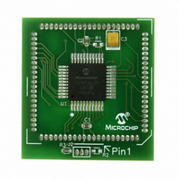
MODULE PLUG-IN PIC18F46J11 PIM
Manufacturer
Microchip Technology
Series
PIC®r
Datasheet
1.MA180023.pdf
(528 pages)
Specifications of MA180023
Accessory Type
Plug-In Module (PIM) - PIC18F46J11
Tool / Board Applications
General Purpose MCU, MPU, DSP, DSC
Mcu Supported Families
PIC18
Supported Devices
Stand-alone Or W/ HPC(DM183022) Or PIC18(DM183032)
Silicon Manufacturer
Microchip
Core Architecture
PIC
Core Sub-architecture
PIC18
Silicon Core Number
PIC18F
Silicon Family Name
PIC18FxxJxx
Lead Free Status / RoHS Status
Lead free / RoHS Compliant
For Use With/related Products
HPC Explorer Board (DM183022) or PIC18 Explorer Board (DM183032)
For Use With
DM183032 - BOARD EXPLORER PICDEM PIC18DM183022 - BOARD DEMO PIC18FXX22 64/80TQFP
Lead Free Status / RoHS Status
Lead free / RoHS Compliant
Available stocks
Company
Part Number
Manufacturer
Quantity
Price
Company:

Part Number:
MA180023
Manufacturer:
Microchip Technology
Quantity:
135


When the RXINC bit is set, the RXADDR register will
automatically increment after each received byte. Auto-
matic receive address increment can be disabled by
clearing the RXINC bit. If RXINC is disabled in
Full-Duplex or Half-Duplex Receive modes, all incom-
ing data bytes on SDI2 will overwrite the same memory
location pointed to by the RXADDR register. After the
SPI DMA transaction has completed, the last received
byte will reside in the memory location pointed to by the
RXADDR register.
The SPI DMA module can be used for either half-duplex
receive only communication, half-duplex transmit only
communication or full-duplex simultaneous transmit and
receive operations. All modes are available for both SPI
master and SPI slave configurations. The DUPLEX0
and DUPLEX1 bits can be used to select the desired
operating mode.
The behavior of the DLYINTEN bit varies greatly
depending on the SPI operating mode. For example
behavior for each of the modes, see Figure 18-3
through Figure 18-6.
SPI Slave mode, DLYINTEN = 1: In this mode, an
SSP2IF interrupt will be generated during a transfer if
the time between successful byte transmission events
is longer than the value set by the DLYCYC<3:0> bits
in the DMACON2 register. This interrupt allows slave
firmware to know that the master device is taking an
unusually large amount of time between byte transmis-
sions. For example, this information may be useful for
implementing
protocols involving time-outs if the bus remains Idle for
too long. When DLYINTEN = 1, the DLYLVL<3:0>
interrupts occur normally according to the selected
setting.
SPI Slave mode, DLYINTEN = 0: In this mode, the
time-out based interrupt is disabled. No additional
SSP2IF interrupt events will be generated by the SPI
DMA module, other than those indicated by the
INTLVL<3:0> bits in the DMACON2 register. In this
mode, always set DLYCYC<3:0> = 0000.
© 2009 Microchip Technology Inc.
application-defined
communication
PIC18F46J11 FAMILY
SPI Master mode, DLYINTEN = 0: The DLYCYC<3:0>
bits in the DMACON2 register determine the amount of
additional inter-byte delay, which is added by the SPI
DMA module during a transfer. The Master mode SS2
output feature may be used.
SPI Master mode, DLYINTEN = 1: The amount of
hardware overhead is slightly reduced in this mode,
and the minimum inter-byte delay is 8 T
9 T
can potentially be used to obtain slightly higher
effective SPI bandwidth. In this mode, the SS2 control
feature cannot be used, and should always be disabled
(DMACON1<7:6> = 00). Additionally, the interrupt
generating hardware (used in Slave mode) remains
active. To avoid extraneous SSP2IF interrupt events,
set the DMACON2 delay bits, DLYCYC<3:0> = 1111,
and ensure that the SPI serial clock rate is no slower
than F
In SPI Master modes, the DMAEN bit is used to enable
the SPI DMA module and to initiate an SPI DMA trans-
action. After user firmware sets the DMAEN bit, the
DMA hardware will begin transmitting and/or receiving
data bytes according to the configuration used. In SPI
Slave modes, setting the DMAEN bit will finish the
initialization steps needed to prepare the SPI DMA
module for communication (which must still be initiated
by the master device).
To avoid possible data corruption, once the DMAEN bit
is set, user firmware should not attempt to modify any
of the MSSP2 or SPI DMA related registers, with the
exception of the INTLVL bits in the DMACON2 register.
If user firmware wants to halt an ongoing DMA transac-
tion, the DMAEN bit can be manually cleared by the
firmware. Clearing the DMAEN bit while a byte is
currently being transmitted will not immediately halt the
byte in progress. Instead, any byte currently in
progress will be completed before the MSSP2 and SPI
DMA modules go back to their Idle conditions. If user
firmware clears the DMAEN bit, the TXADDR,
RXADDR and DMABC registers will no longer update,
and the DMA module will no longer make any
additional read or writes to SRAM; therefore, state
information can be lost.
CY
for F
OSC
/64.
OSC
/16 and 15 T
CY
for F
DS39932C-page 277
OSC
/64. This mode
CY
for F
OSC
/4,
Related parts for MA180023
Image
Part Number
Description
Manufacturer
Datasheet
Request
R

Part Number:
Description:
Manufacturer:
Microchip Technology Inc.
Datasheet:
Part Number:
Description:
Manufacturer:
Microchip Technology Inc.
Datasheet:
Part Number:
Description:
Manufacturer:
Microchip Technology Inc.
Datasheet:
Part Number:
Description:
Manufacturer:
Microchip Technology Inc.
Datasheet:
Part Number:
Description:
Manufacturer:
Microchip Technology Inc.
Datasheet:
Part Number:
Description:
Manufacturer:
Microchip Technology Inc.
Datasheet:
Part Number:
Description:
Manufacturer:
Microchip Technology Inc.
Datasheet:
Part Number:
Description:
Manufacturer:
Microchip Technology Inc.
Datasheet: