MA180023 Microchip Technology, MA180023 Datasheet - Page 352
MA180023
Manufacturer Part Number
MA180023
Description
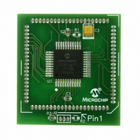
MODULE PLUG-IN PIC18F46J11 PIM
Manufacturer
Microchip Technology
Series
PIC®r
Datasheet
1.MA180023.pdf
(528 pages)
Specifications of MA180023
Accessory Type
Plug-In Module (PIM) - PIC18F46J11
Tool / Board Applications
General Purpose MCU, MPU, DSP, DSC
Mcu Supported Families
PIC18
Supported Devices
Stand-alone Or W/ HPC(DM183022) Or PIC18(DM183032)
Silicon Manufacturer
Microchip
Core Architecture
PIC
Core Sub-architecture
PIC18
Silicon Core Number
PIC18F
Silicon Family Name
PIC18FxxJxx
Lead Free Status / RoHS Status
Lead free / RoHS Compliant
For Use With/related Products
HPC Explorer Board (DM183022) or PIC18 Explorer Board (DM183032)
For Use With
DM183032 - BOARD EXPLORER PICDEM PIC18DM183022 - BOARD DEMO PIC18FXX22 64/80TQFP
Lead Free Status / RoHS Status
Lead free / RoHS Compliant
Available stocks
Company
Part Number
Manufacturer
Quantity
Price
Company:

Part Number:
MA180023
Manufacturer:
Microchip Technology
Quantity:
135


PIC18F46J11 FAMILY
20.5
Figure 20-3 displays the operation of the A/D Converter
after the GO/DONE bit has been set and the
ACQT<2:0> bits are cleared. A conversion is started
after the following instruction to allow entry into Sleep
mode before the conversion begins.
Figure 20-4 displays the operation of the A/D Converter
after the GO/DONE bit has been set, the ACQT<2:0>
bits are set to ‘010’ and a 4 T
been selected before the conversion starts.
Clearing the GO/DONE bit during a conversion will
abort the current conversion. The A/D Result register
pair will NOT be updated with the partially completed
A/D
ADRESH:ADRESL registers will continue to contain
the value of the last completed conversion (or the last
value written to the ADRESH:ADRESL registers).
After the A/D conversion is completed or aborted, a
2 T
started. After this wait, acquisition on the selected
channel is automatically started.
FIGURE 20-3:
FIGURE 20-4:
DS39932C-page 352
Note:
(Holding capacitor continues
acquiring input)
AD
Set GO/DONE bit
wait is required before the next acquisition can be
1
conversion
A/D Conversions
T
T
Set GO/DONE bit
CY
Automatic
Acquisition
Time
ACQT
Holding capacitor is disconnected from analog input (typically 100 ns)
The GO/DONE bit should NOT be set in
the same instruction that turns on the A/D.
2
- T
AD
Cycles
Conversion starts
T
3
AD
sample.
A/D CONVERSION T
A/D CONVERSION T
1 T
4
AD
b9
2 T
Conversion starts
(Holding capacitor is disconnected)
AD
1
This
AD
acquisition time has
b8
3 T
b9
2
AD
means
Next Q4: ADRESH:ADRESL are loaded, GO/DONE bit is cleared,
b7
Next Q4: ADRESH/ADRESL are loaded, GO/DONE bit is cleared,
4 T
b8
3
AD
AD
AD
b6
5 T
CYCLES (ACQT<2:0> = 000, T
CYCLES (ACQT<2:0> = 010, T
ADIF bit is set, holding capacitor is reconnected to analog input.
the
ADIF bit is set, holding capacitor is connected to analog input.
b7
4
AD
b5
6 T
T
5
b6
AD
AD
b4
7 T
Cycles
20.6
An A/D conversion can be started by the Special Event
Trigger of the ECCP2 module. This requires that the
CCP2M<3:0> bits (CCP2CON<3:0>) be programmed
as ‘1011’ and that the A/D module is enabled (ADON
bit is set). When the trigger occurs, the GO/DONE bit
will be set, starting the A/D acquisition and conversion,
and the Timer1 (or Timer3) counter will be reset to zero.
Timer1 (or Timer3) is reset to automatically repeat the
A/D acquisition period with minimal software overhead
(moving ADRESH/ADRESL to the desired location).
The appropriate analog input channel must be selected
and the minimum acquisition period is either timed by
the user, or an appropriate T
the Special Event Trigger sets the GO/DONE bit (starts
a conversion).
If the A/D module is not enabled (ADON is cleared), the
Special Event Trigger will be ignored by the A/D module
but will still reset the Timer1 (or Timer3) counter.
b5
6
AD
b3
8
Use of the ECCP2 Trigger
b4
T
7
AD
b2
9 T
b3
8
AD
b1
10
ACQ
ACQ
T
b2
9
AD
© 2009 Microchip Technology Inc.
b0
11
ACQ
= 0)
= 4 T
10
b1
time is selected before
AD
b0
)
11
Related parts for MA180023
Image
Part Number
Description
Manufacturer
Datasheet
Request
R

Part Number:
Description:
Manufacturer:
Microchip Technology Inc.
Datasheet:
Part Number:
Description:
Manufacturer:
Microchip Technology Inc.
Datasheet:
Part Number:
Description:
Manufacturer:
Microchip Technology Inc.
Datasheet:
Part Number:
Description:
Manufacturer:
Microchip Technology Inc.
Datasheet:
Part Number:
Description:
Manufacturer:
Microchip Technology Inc.
Datasheet:
Part Number:
Description:
Manufacturer:
Microchip Technology Inc.
Datasheet:
Part Number:
Description:
Manufacturer:
Microchip Technology Inc.
Datasheet:
Part Number:
Description:
Manufacturer:
Microchip Technology Inc.
Datasheet: