MA180023 Microchip Technology, MA180023 Datasheet - Page 358
MA180023
Manufacturer Part Number
MA180023
Description
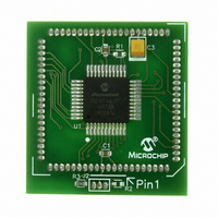
MODULE PLUG-IN PIC18F46J11 PIM
Manufacturer
Microchip Technology
Series
PIC®r
Datasheet
1.MA180023.pdf
(528 pages)
Specifications of MA180023
Accessory Type
Plug-In Module (PIM) - PIC18F46J11
Tool / Board Applications
General Purpose MCU, MPU, DSP, DSC
Mcu Supported Families
PIC18
Supported Devices
Stand-alone Or W/ HPC(DM183022) Or PIC18(DM183032)
Silicon Manufacturer
Microchip
Core Architecture
PIC
Core Sub-architecture
PIC18
Silicon Core Number
PIC18F
Silicon Family Name
PIC18FxxJxx
Lead Free Status / RoHS Status
Lead free / RoHS Compliant
For Use With/related Products
HPC Explorer Board (DM183022) or PIC18 Explorer Board (DM183032)
For Use With
DM183032 - BOARD EXPLORER PICDEM PIC18DM183022 - BOARD DEMO PIC18FXX22 64/80TQFP
Lead Free Status / RoHS Status
Lead free / RoHS Compliant
Available stocks
Company
Part Number
Manufacturer
Quantity
Price
Company:

Part Number:
MA180023
Manufacturer:
Microchip Technology
Quantity:
135


PIC18F46J11 FAMILY
21.2
A single comparator is shown in Figure 21-2, along with
the relationship between the analog input levels and
the digital output. When the analog input at V
than the analog input, V
tor is a digital low level. When the analog input at V
is greater than the analog input, V
comparator is a digital high level. The shaded areas of
the output of the comparator in Figure 21-2 represent
the uncertainty due to input offsets and response time.
FIGURE 21-2:
FIGURE 21-3:
DS39932C-page 358
V
V
Output
IN
IN
-
+
V
V
IN
IN
Comparator Operation
+
-
VA
R
S
Legend:
+
–
< 10k
SINGLE COMPARATOR
COMPARATOR ANALOG INPUT MODEL
IN
-, the output of the compara-
A
IN
C
V
I
R
R
VA
LEAKAGE
C
5 pF
PIN
T
IC
S
IN
PIN
-, the output of the
Output
= Input Capacitance
= Threshold Voltage
= Leakage Current at the pin due to various junctions
= Interconnect Resistance
= Source Impedance
= Analog Voltage
IN
+ is less
IN
V
+
DD
V
V
T
T
= 0.6V
= 0.6V
21.3
Response time is the minimum time, after selecting a
new reference voltage or input source, before the
comparator output has a valid level. The response time
of the comparator differs from the settling time of the
voltage reference. Therefore, both of these times must
be considered when determining the total response to
a comparator input change. Otherwise, the maximum
delay of the comparators should be used (see
Section 28.0 “Electrical Characteristics”).
21.4
Figure 21-3 provides a simplified circuit for an analog
input. Since the analog pins are connected to a digital
output, they have reverse biased diodes to V
V
and V
by more than 0.6V in either direction, one of the diodes
is forward biased and a latch-up condition may occur.
A maximum source impedance of 10 kΩ is
recommended for the analog sources. Any external
component connected to an analog input pin, such as
a capacitor or a Zener diode, should have very little
leakage current.
SS
. The analog input, therefore, must be between V
DD
. If the input voltage deviates from this range
Comparator
Analog Input Connection
Considerations
I
±100 nA
V
LEAKAGE
SS
R
IC
© 2009 Microchip Technology Inc.
Response Time
Comparator
Input
DD
and
SS
Related parts for MA180023
Image
Part Number
Description
Manufacturer
Datasheet
Request
R

Part Number:
Description:
Manufacturer:
Microchip Technology Inc.
Datasheet:
Part Number:
Description:
Manufacturer:
Microchip Technology Inc.
Datasheet:
Part Number:
Description:
Manufacturer:
Microchip Technology Inc.
Datasheet:
Part Number:
Description:
Manufacturer:
Microchip Technology Inc.
Datasheet:
Part Number:
Description:
Manufacturer:
Microchip Technology Inc.
Datasheet:
Part Number:
Description:
Manufacturer:
Microchip Technology Inc.
Datasheet:
Part Number:
Description:
Manufacturer:
Microchip Technology Inc.
Datasheet:
Part Number:
Description:
Manufacturer:
Microchip Technology Inc.
Datasheet: