MA180023 Microchip Technology, MA180023 Datasheet - Page 451
MA180023
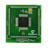
Manufacturer Part Number
MA180023
Description
MODULE PLUG-IN PIC18F46J11 PIM
Manufacturer
Microchip Technology
Series
PIC®r
Datasheet
1.MA180023.pdf
(528 pages)
Specifications of MA180023
Accessory Type
Plug-In Module (PIM) - PIC18F46J11
Tool / Board Applications
General Purpose MCU, MPU, DSP, DSC
Mcu Supported Families
PIC18
Supported Devices
Stand-alone Or W/ HPC(DM183022) Or PIC18(DM183032)
Silicon Manufacturer
Microchip
Core Architecture
PIC
Core Sub-architecture
PIC18
Silicon Core Number
PIC18F
Silicon Family Name
PIC18FxxJxx
Lead Free Status / RoHS Status
Lead free / RoHS Compliant
For Use With/related Products
HPC Explorer Board (DM183022) or PIC18 Explorer Board (DM183032)
For Use With
DM183032 - BOARD EXPLORER PICDEM PIC18DM183022 - BOARD DEMO PIC18FXX22 64/80TQFP
Lead Free Status / RoHS Status
Lead free / RoHS Compliant
Available stocks
Company
Part Number
Manufacturer
Quantity
Price
Company:

Part Number:
MA180023
Manufacturer:
Microchip Technology
Quantity:
135


CALLW
Syntax:
Operands:
Operation:
Status Affected:
Encoding:
Description
Words:
Cycles:
Example:
© 2009 Microchip Technology Inc.
Q Cycle Activity:
Before Instruction
After Instruction
operation
Decode
No
PC
PCLATH =
PCLATU =
W
PC
TOS
PCLATH =
PCLATU =
W
Q1
=
=
=
=
=
operation
Subroutine Call using WREG
CALLW
None
(PC + 2) → TOS,
(W) → PCL,
(PCLATH) → PCH,
(PCLATU) → PCU
None
First, the return address (PC + 2) is
pushed onto the return stack. Next, the
contents of W are written to PCL; the
existing value is discarded. Then, the
contents of PCLATH and PCLATU are
latched into PCH and PCU, respec-
tively. The second cycle is executed as
a NOP instruction while the new next
instruction is fetched.
Unlike CALL, there is no option to
update W, STATUS or BSR.
1
2
HERE
WREG
Read
0000
No
Q2
address (HERE)
10h
00h
06h
001006h
address (HERE + 2)
10h
00h
06h
CALLW
0000
Push PC to
operation
stack
No
Q3
0001
operation
operation
No
No
Q4
0100
PIC18F46J11 FAMILY
MOVSF
Syntax:
Operands:
Operation:
Status Affected:
Encoding:
1st word (source)
2nd word (destin.)
Description:
Words:
Cycles:
Example:
Q Cycle Activity:
Before Instruction
After Instruction
Decode
Decode
FSR2
Contents
of 85h
REG2
FSR2
Contents
of 85h
REG2
Q1
source addr
No dummy
Determine
operation
Move Indexed to f
MOVSF [z
0 ≤ z
0 ≤ f
((FSR2) + z
None
The contents of the source register are
moved to destination register ‘f
actual address of the source register is
determined by adding the 7-bit literal
offset ‘z
of FSR2. The address of the destina-
tion register is specified by the 12-bit lit-
eral ‘f
addresses can be anywhere in the
4096-byte data space (000h to FFFh).
The MOVSF instruction cannot use the
PCL, TOSU, TOSH or TOSL as the
destination register.
If the resultant source address points to
an Indirect Addressing register, the
value returned will be 00h.
2
2
MOVSF
read
1110
1111
No
Q2
=
=
=
=
=
=
d
s
d
≤ 4095
≤ 127
’ in the second word. Both
s
’, in the first word, to the value
80h
33h
11h
80h
33h
33h
[05h], REG2
s
s
1011
ffff
source addr
], f
) → f
Determine
operation
d
No
Q3
d
DS39932C-page 451
0zzz
ffff
source reg
register ‘f’
(dest)
Read
Write
d
Q4
zzzz
ffff
’. The
s
d
Related parts for MA180023
Image
Part Number
Description
Manufacturer
Datasheet
Request
R

Part Number:
Description:
Manufacturer:
Microchip Technology Inc.
Datasheet:
Part Number:
Description:
Manufacturer:
Microchip Technology Inc.
Datasheet:
Part Number:
Description:
Manufacturer:
Microchip Technology Inc.
Datasheet:
Part Number:
Description:
Manufacturer:
Microchip Technology Inc.
Datasheet:
Part Number:
Description:
Manufacturer:
Microchip Technology Inc.
Datasheet:
Part Number:
Description:
Manufacturer:
Microchip Technology Inc.
Datasheet:
Part Number:
Description:
Manufacturer:
Microchip Technology Inc.
Datasheet:
Part Number:
Description:
Manufacturer:
Microchip Technology Inc.
Datasheet: