RDK-201 Power Integrations, RDK-201 Datasheet - Page 11
RDK-201
Manufacturer Part Number
RDK-201
Description
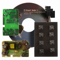
KIT REF DESIGN LINKSWITCH-CV
Manufacturer
Power Integrations
Series
LinkSwitch®-CVr
Type
MOSFET & Power Driverr
Specifications of RDK-201
Main Purpose
AC/DC, Primary Side
Outputs And Type
1, Isolated
Power - Output
6W
Voltage - Output
5V
Current - Output
1.2A
Voltage - Input
90 ~ 265VAC
Regulator Topology
Flyback
Board Type
Fully Populated
Utilized Ic / Part
LNK626
Product
Power Management Modules
Lead Free Status / RoHS Status
Lead free / RoHS Compliant
Frequency - Switching
-
Lead Free Status / Rohs Status
Lead free / RoHS Compliant
For Use With/related Products
LNK62x
Other names
596-1266


www.powerint.com
Thermal Resistance
Thermal Resistance: P Package:
Absolute Maximum Ratings
DRAIN Voltage .................................. ......... ..............-0.3 V to 700 V
DRAIN Peak Current: LNK623 ......................... 400 (600) mA
Peak Negative Pulsed DRAIN Current ................... ...... -100 mA
Feedback Voltage ................................................. ....... -0.3 V to 9 V
Feedback Current ................................................. .............. 100 mA
BYPASS Pin Voltage ..................................... ............. -0.3 V to 9 V
Storage Temperature ...................................... ..... -65 °C to 150 °C
Operating Junction Temperature.........................-40 °C to 150 °C
Lead Temperature
Output Frequency
Frequency Jitter
Ratio of Output
Frequency at Auto-RST
Maximum Duty Cycle
Feedback Pin Voltage
Feedback Pin Voltage
Temperature
Coeffi cient
Feedback Pin Voltage
at Turn-Off Threshold
Power Coeffi cient
Control Functions
Parameter
(θ
(θ
(θ
(θ
JA
JC
JA
JC
(3)
) ....................................70 °C/W
)
)
.................................................................260 °C
(1)
.....................................100 °C/W
(1)
D Package:
............................................... ......... 11 °C/W
.......................... ...........................30 °C/W
LNK624 ......................... 400 (600) mA
LNK625 ..........................528 (790) mA
LNK626 ........................720 (1080) mA
Symbol
f
DC
V
TC
(1,4)
OSC(AR)
V
f
FB(AR)
OSC
I
FBth
2
MAX
VFB
f
I
I
2
2
See Figure 15,
T
f = I
f = I
J
C
T
SOURCE = 0 V; T
= 25 °C, V
J
BP
2
2
= 25 °C
LIMIT(TYP)
LIMIT(TYP)
= 1 μF
Average Frequency, T
Peak-Peak Jitter Compared to
(Unless Otherwise Specifi ed)
Relative to f
(2)
(2)
; 60 °C/W
(Note 2,3) T
; 80 °C/W
× f
× f
FB
OSC(TYP)
OSC(TYP)
Conditions
= V
T
J
= 25 °C
FBth
OSC
LNK625P, LNK625D
LNK626P, LNK626D
(3)
(3)
(4)
(4)
(4)
(4)
(2)
J
J
LNK623-624P
LNK623-624D
(See Note 3)
= -40 to 125 °C
= 25 °C
Notes:
1. All voltages referenced to SOURCE, T
2. Duration not to exceed 2 msec.
3. 1/16 in. from case for 5 seconds.
4. The higher peak DRAIN current is allowed while the DRAIN
5. Maximum ratings specifi ed may be applied, one at a time
Notes:
1. Measured on pin 8 (SOURCE) close to plastic interface.
2. Soldered to 0.36 sq. in. (232 mm
3. Soldered to 1 sq. in. (645 mm
LNK623/6P
LNK623/6D
T
T
J
without causing permanent damage to the product.
periods of time may affect product reliability.
voltage is simultaneously less than 400 V.
Exposure to Absolute Maximum ratings for extended
LNK623/6
= 25 °C
J
J
= 25 °C
= 25 °C
0.9 × I
0.9 × I
1.815
1.855
1.835
1.775
Min
93
54
2
2
f
f
2
), 2 oz. (610 g/m
1.840
1.880
1.860
1.800
-0.01
2
1.45
Typ
100
), 2 oz. (610 g/m
±7
80
I
I
LNK623-626
2
2
f
f
A
= 25 °C.
1.17 × I
1.21 × I
1.865
1.905
1.885
1.825
Max
106
2
) copper clad.
2
) copper clad.
2
2
f
f
Units
%/°C
A
Rev. E 09/09
kHz
%
%
%
2
V
V
Hz
11
Related parts for RDK-201
Image
Part Number
Description
Manufacturer
Datasheet
Request
R

Part Number:
Description:
KIT REF DESIGN TOP HX FOR TOP258
Manufacturer:
Power Integrations
Datasheet:

Part Number:
Description:
KIT REF DESIGN LINKSWITCH 2
Manufacturer:
Power Integrations
Datasheet:

Part Number:
Description:
KIT REF DESIGN 1.2W PS TN FAMILY
Manufacturer:
Power Integrations
Datasheet:

Part Number:
Description:
KIT REF DESIGN 36-72W MOTOR DRVR
Manufacturer:
Power Integrations
Datasheet:

Part Number:
Description:
KIT REF DESIGN FOR LNK457D
Manufacturer:
Power Integrations
Datasheet:

Part Number:
Description:
REFERENCE DESIGN LINKSWITCH-PH
Manufacturer:
Power Integrations
Datasheet:

Part Number:
Description:
Specifications: Manufacturer: Power Integrations ; Output Voltage: 380 VDC ; Input / Supply Voltage (Max): 264 VAC ; Input / Supply Voltage (Min): 90 VAC ; Mounting Style: Through Hole ; Output Current: 0.913 A ; Output Power: 347 W
Manufacturer:
Power Integrations, Inc.

Part Number:
Description:
Power Management Modules & Development Tools TOPSwitch-JX REF. DESIGN KIT
Manufacturer:
Power Integrations
Datasheet:
Part Number:
Description:
Power Management IC Development Tools REF DESIGN RDR-292 PFF LED STREET LIGHT
Manufacturer:
Power Integrations

Part Number:
Description:
KIT REF DESIGN FOR LNK403EG
Manufacturer:
Power Integrations
Datasheet:

Part Number:
Description:
KIT REF DESIGN FOR LNK406EG
Manufacturer:
Power Integrations
Datasheet:

Part Number:
Description:
KIT REF DESIGN DG CAPZERO
Manufacturer:
Power Integrations
Datasheet:

Part Number:
Description:
KIT REF DESIGN PFS762HG
Manufacturer:
Power Integrations
Datasheet:
Part Number:
Description:
Specifications: Family: Eval Boards - DC/DC & AC/DC (Off-Line) SMPS ; Series: HiperLCS™ ; Main Purpose: DC/DC, Step Down ; Outputs and Type: 1, Isolated ; Power - Output: 150W ; Voltage - Output: 24V ; Current - Output: 6.25A ; Voltage - Input:
Manufacturer:
Power Integrations, Inc.
Datasheet:

Part Number:
Description:
KIT REFERENCE DESIGN W/TN376PN
Manufacturer:
Power Integrations
Datasheet: