RDK-201 Power Integrations, RDK-201 Datasheet - Page 8
RDK-201
Manufacturer Part Number
RDK-201
Description
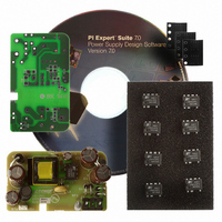
KIT REF DESIGN LINKSWITCH-CV
Manufacturer
Power Integrations
Series
LinkSwitch®-CVr
Type
MOSFET & Power Driverr
Specifications of RDK-201
Main Purpose
AC/DC, Primary Side
Outputs And Type
1, Isolated
Power - Output
6W
Voltage - Output
5V
Current - Output
1.2A
Voltage - Input
90 ~ 265VAC
Regulator Topology
Flyback
Board Type
Fully Populated
Utilized Ic / Part
LNK626
Product
Power Management Modules
Lead Free Status / RoHS Status
Lead free / RoHS Compliant
Frequency - Switching
-
Lead Free Status / Rohs Status
Lead free / RoHS Compliant
For Use With/related Products
LNK62x
Other names
596-1266


Rev. E 09/09
Drain Clamp
Recommended Clamp Circuits
Components R1, R2, C3, VR1 and D5 in fi gure 4 comprise the
clamp. This circuit is preferred when the primary leakage
inductance is greater than 125 μH to reduce drain voltage
overshoot or ringing present on the feedback winding. For best
output regulation, the feedback voltage must settle to within 1%
at 2.1 μs from the turn off of the primary MOSFET. This requires
careful selection of the clamp circuit components. The voltage of
VR1 is selected to be ~20% above the refl ected output voltage
(V
conduction during the fl yback voltage interval when the output
diode is conducting. The value of R1 should be the largest value
that results in acceptable settling of the feedback pin voltage and
peak drain voltage. Making R1 too large will increase the
discharge time of C3 and degrade regulation. Resistor R2
dampens the leakage inductance ring. The value must be large
enough to dampen the ring in the required time but must not be
too large to cause the drain voltage to exceed 680 V.
If the primary leakage inductance is less than 125 μH, VR1 can
be eliminated and the value of R1 increased. A value of 470 kΩ
with an 820 pF capacitor is a recommended starting point.
Verify that the peak drain voltage is less than 680 V under all
line and load conditions. Verify the feedback winding settles to
an acceptable limit for good line and load regulation.
Effect of Fast (500 ns) versus Slow (2 μs) Recovery
Diodes in Clamp Circuit on Pulse Grouping and Output
Ripple.
A slow reverse recovery diode reduces the feedback voltage
ringing. The amplitude of ringing with a fast diode represents
8% error in Figure 10.
Figure 9.
OR
8
). This is to clip any turn off spike on the drain but avoid
RCD Clamp, Low Power or Low Leakage Inductance Designs.
LNK623-626
R
C2
R
D
C1
C1
PI-5107-110308
C
C1
RCD Clamp With Zener Bleed. High Power or High Leakage Inductance Designs.
Figure 10. Effect of Clamp Diode on Feedback Pin Settling. Clamp Circuit (top).
Black Trace: D
Gray Trace: D
Feedback Pin Voltage (bottom).
C1
C1
is a 1N4007G (standard recovery, trr = 2 us)
is a FR107 (fast type, trr = 500 ns)
D
R
C2
R
C2
C2
D
R
C1
C1
R
D
C1
C1
PI-5108-110308
C
PI-5107-110308
C1
C
C1
www.powerint.com
Related parts for RDK-201
Image
Part Number
Description
Manufacturer
Datasheet
Request
R

Part Number:
Description:
KIT REF DESIGN TOP HX FOR TOP258
Manufacturer:
Power Integrations
Datasheet:

Part Number:
Description:
KIT REF DESIGN LINKSWITCH 2
Manufacturer:
Power Integrations
Datasheet:

Part Number:
Description:
KIT REF DESIGN 1.2W PS TN FAMILY
Manufacturer:
Power Integrations
Datasheet:

Part Number:
Description:
KIT REF DESIGN 36-72W MOTOR DRVR
Manufacturer:
Power Integrations
Datasheet:

Part Number:
Description:
KIT REF DESIGN FOR LNK457D
Manufacturer:
Power Integrations
Datasheet:

Part Number:
Description:
REFERENCE DESIGN LINKSWITCH-PH
Manufacturer:
Power Integrations
Datasheet:

Part Number:
Description:
Specifications: Manufacturer: Power Integrations ; Output Voltage: 380 VDC ; Input / Supply Voltage (Max): 264 VAC ; Input / Supply Voltage (Min): 90 VAC ; Mounting Style: Through Hole ; Output Current: 0.913 A ; Output Power: 347 W
Manufacturer:
Power Integrations, Inc.

Part Number:
Description:
Power Management Modules & Development Tools TOPSwitch-JX REF. DESIGN KIT
Manufacturer:
Power Integrations
Datasheet:
Part Number:
Description:
Power Management IC Development Tools REF DESIGN RDR-292 PFF LED STREET LIGHT
Manufacturer:
Power Integrations

Part Number:
Description:
KIT REF DESIGN FOR LNK403EG
Manufacturer:
Power Integrations
Datasheet:

Part Number:
Description:
KIT REF DESIGN FOR LNK406EG
Manufacturer:
Power Integrations
Datasheet:

Part Number:
Description:
KIT REF DESIGN DG CAPZERO
Manufacturer:
Power Integrations
Datasheet:

Part Number:
Description:
KIT REF DESIGN PFS762HG
Manufacturer:
Power Integrations
Datasheet:
Part Number:
Description:
Specifications: Family: Eval Boards - DC/DC & AC/DC (Off-Line) SMPS ; Series: HiperLCS™ ; Main Purpose: DC/DC, Step Down ; Outputs and Type: 1, Isolated ; Power - Output: 150W ; Voltage - Output: 24V ; Current - Output: 6.25A ; Voltage - Input:
Manufacturer:
Power Integrations, Inc.
Datasheet:

Part Number:
Description:
KIT REFERENCE DESIGN W/TN376PN
Manufacturer:
Power Integrations
Datasheet: