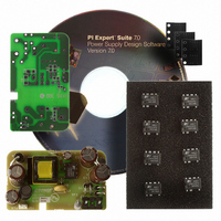
RDK-201 Power Integrations, RDK-201 Datasheet - Page 9

RDK-201
Manufacturer Part Number
RDK-201
Description
KIT REF DESIGN LINKSWITCH-CV
Manufacturer
Power Integrations
Series
LinkSwitch®-CVr
Type
MOSFET & Power Driverr
Specifications of RDK-201
Main Purpose
AC/DC, Primary Side
Outputs And Type
1, Isolated
Power - Output
6W
Voltage - Output
5V
Current - Output
1.2A
Voltage - Input
90 ~ 265VAC
Regulator Topology
Flyback
Board Type
Fully Populated
Utilized Ic / Part
LNK626
Product
Power Management Modules
Lead Free Status / RoHS Status
Lead free / RoHS Compliant
Frequency - Switching
-
Lead Free Status / Rohs Status
Lead free / RoHS Compliant
For Use With/related Products
LNK62x
Other names
596-1266
Clampless Designs
Clampless designs rely solely on the drain node capacitance to
limit the leakage inductance induced peak drain-to-source
voltage. Therefore the maximum AC input line voltage, the value
of V
inductance and peak primary current), and the primary winding
capacitance determine the peak drain voltage. With no signifi -
cant dissipative element present, as is the case with an external
clamp, the longer duration of the leakage inductance ringing can
increase EMI.
The following requirements are recommended for a universal
input or 230 VAC only Clampless design:
1. Clampless designs should only be used for P
2. For designs with P
3. For designs with P
4. Ensure that worst-case, high line, peak drain voltage is below
V
output diode forward voltage drop that is refl ected to the primary
via the turns ratio of the transformer during the diode conduction
time. The V
to determine the peak drain voltage.
Pulse Grouping
Pulse grouping is defi ned as 6 or more consecutive pulses
followed by two or more timing state changes. The effect of
pulse grouping is increased output voltage ripple. This is
Figure 11. Not Pulse Grouping (<5 Consecutive Switching Cycles).
www.powerint.com
OR
V
to ensure adequate primary intra-winding capacitance in the
range of 25 pF to 50 pF. A bias winding must be added to
the transformer using a standard recovery rectifi er diode
(1N4003– 1N4007) to act as a clamp. This bias winding may
also be used to externally power the device by connecting a
resistor from the bias winding capacitor to the BYPASS pin.
This inhibits the internal high-voltage current source,
reducing device dissipation and no-load consumption.
and an external RCD or Zener clamp should be used.
the BV
≤650 V to allow margin for design variation.
Top Trace: Drain Waveform (200 V/div)
Top Trace: Drain Waveform (200 V/div)
Bottom Trace: Output Ripple Voltage (50 mV/div)
Bottom Trace: Output Ripple Voltage (50 mV/div)
OR
(Refl ected Output Voltage), is the secondary output plus
OR
, the leakage inductance energy, (a function of leakage
of ≤90 V
DSS
OR
specifi cation of the internal MOSFET and ideally
adds to the DC bus voltage and the leakage spike
O
O
>5 W, Clampless designs are not practical
≤5 W, a two-layer primary must be used
O
≤5 W using a
Pulse Grouping (>5 Consecutive Switching Cycles).
shown on the right of Figure 11 where pulse grouping has
caused an increase in the output ripple.
To eliminate group pulsing verify that the feedback signal settles
within 2.1 μs from the turn off of the internal MOSFET. A Zener
diode in the clamp circuit may be needed to achieve the desired
settling time. If the settling time is satisfactory, then a RC
network across R
necessary.
The value of R (R5 in the Figure 12) should be an order of
magnitude greater than R
R×C = 32 μs where C is C5 in Figure 12.
Quick Design Checklist
As with any power supply design, all LinkSwitch-CV designs
should be verifi ed on the bench to make sure that component
specifi cations are not exceeded under worst-case conditions.
Figure 12. RC Network Across R
Split Screen with Bottom Screen Zoom
Split Screen with Bottom Screen Zoom
Top Trace: Drain Waveform (200 V/div)
Top Trace: Drain Waveform (200 V/div)
Bottom Trace: Output Ripple Voltage (50 mV/div)
Bottom Trace: Output Ripple Voltage (50 mV/div)
LinkSwitch-CV
LNK626PG
50 V
1 F
C4
LOWER
U1
(R6) of the feedback resistors is
LOWER
6.2 k
R4
BOTTOM
and selected such that
(R6) to Reduce Pulse Grouping.
LNK623-626
47 k
1/8 W
680 pF
R5
50 V
C5
5
4
2
4.02 k
1%
R6
1N4148
D6
PI-5268-110608
6.34 k
10 F
50 V
1%
R3
C6
Rev. E 09/09
9


