RDK-201 Power Integrations, RDK-201 Datasheet - Page 2
RDK-201
Manufacturer Part Number
RDK-201
Description
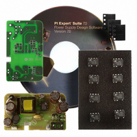
KIT REF DESIGN LINKSWITCH-CV
Manufacturer
Power Integrations
Series
LinkSwitch®-CVr
Type
MOSFET & Power Driverr
Specifications of RDK-201
Main Purpose
AC/DC, Primary Side
Outputs And Type
1, Isolated
Power - Output
6W
Voltage - Output
5V
Current - Output
1.2A
Voltage - Input
90 ~ 265VAC
Regulator Topology
Flyback
Board Type
Fully Populated
Utilized Ic / Part
LNK626
Product
Power Management Modules
Lead Free Status / RoHS Status
Lead free / RoHS Compliant
Frequency - Switching
-
Lead Free Status / Rohs Status
Lead free / RoHS Compliant
For Use With/related Products
LNK62x
Other names
596-1266


Rev. E 09/09
Figure 2
Pin Functional Description
DRAIN (D) Pin:
This pin is the power MOSFET drain connection. It provides
internal operating current for both start-up and steady-state
operation.
BYPASS (BP) Pin:
This pin is the connection point for an external bypass capacitor
for the internally generated 6 V supply.
FEEDBACK (FB) Pin:
During normal operation, switching of the power MOSFET is
controlled by this pin. This pin senses the AC voltage on the
bias winding. This control input regulates the output voltage
based on the fl yback voltage of the bias winding.
SOURCE (S) Pin:
This pin is internally connected to the output MOSFET source
for high voltage power and control circuit common returns.
2
FEEDBACK
SOURCE
BYPASS
Functional Block Diagram.
(BP)
(FB)
(S)
LNK623-626
6.5 V
V
TH
+
FB
-
t
SAMPLE-OUT
DC
MAX
I
LIM
OSCILLATOR
Auto-Restart
Open-Loop
FAULT
D
Q
OUT
FB
I
LIM
DC
MACHINE
MAX
STATE
Drive
Reset
Figure 3.
V
SHUTDOWN
ILIMIT
BP
THERMAL
FB
P Package (DIP-8C)
D
Current Limit
Comparator
t
1
2
4
Pin Confi guration.
SAMPLE-OUT
6 V
5 V
+
-
3a
V
+
-
ILIMIT
SAMPLE
BLANKING
DELAY
LEADING
8
7
6
5
EDGE
S
S
S
S
REGULATOR
6 V
D Package (SO-8C)
FB
BP
D
1
2
4
www.powerint.com
3b
SOURCE
DRAIN
PI-5198-071608
(D)
(S)
8
PI-5197-110408
7
6
5
S
S
S
S
Related parts for RDK-201
Image
Part Number
Description
Manufacturer
Datasheet
Request
R

Part Number:
Description:
KIT REF DESIGN TOP HX FOR TOP258
Manufacturer:
Power Integrations
Datasheet:

Part Number:
Description:
KIT REF DESIGN LINKSWITCH 2
Manufacturer:
Power Integrations
Datasheet:

Part Number:
Description:
KIT REF DESIGN 1.2W PS TN FAMILY
Manufacturer:
Power Integrations
Datasheet:

Part Number:
Description:
KIT REF DESIGN 36-72W MOTOR DRVR
Manufacturer:
Power Integrations
Datasheet:

Part Number:
Description:
KIT REF DESIGN FOR LNK457D
Manufacturer:
Power Integrations
Datasheet:

Part Number:
Description:
REFERENCE DESIGN LINKSWITCH-PH
Manufacturer:
Power Integrations
Datasheet:

Part Number:
Description:
Specifications: Manufacturer: Power Integrations ; Output Voltage: 380 VDC ; Input / Supply Voltage (Max): 264 VAC ; Input / Supply Voltage (Min): 90 VAC ; Mounting Style: Through Hole ; Output Current: 0.913 A ; Output Power: 347 W
Manufacturer:
Power Integrations, Inc.

Part Number:
Description:
Power Management Modules & Development Tools TOPSwitch-JX REF. DESIGN KIT
Manufacturer:
Power Integrations
Datasheet:
Part Number:
Description:
Power Management IC Development Tools REF DESIGN RDR-292 PFF LED STREET LIGHT
Manufacturer:
Power Integrations

Part Number:
Description:
KIT REF DESIGN FOR LNK403EG
Manufacturer:
Power Integrations
Datasheet:

Part Number:
Description:
KIT REF DESIGN FOR LNK406EG
Manufacturer:
Power Integrations
Datasheet:

Part Number:
Description:
KIT REF DESIGN DG CAPZERO
Manufacturer:
Power Integrations
Datasheet:

Part Number:
Description:
KIT REF DESIGN PFS762HG
Manufacturer:
Power Integrations
Datasheet:
Part Number:
Description:
Specifications: Family: Eval Boards - DC/DC & AC/DC (Off-Line) SMPS ; Series: HiperLCS™ ; Main Purpose: DC/DC, Step Down ; Outputs and Type: 1, Isolated ; Power - Output: 150W ; Voltage - Output: 24V ; Current - Output: 6.25A ; Voltage - Input:
Manufacturer:
Power Integrations, Inc.
Datasheet:

Part Number:
Description:
KIT REFERENCE DESIGN W/TN376PN
Manufacturer:
Power Integrations
Datasheet: