CYIL1SE0300-EVAL Cypress Semiconductor Corp, CYIL1SE0300-EVAL Datasheet
CYIL1SE0300-EVAL
Specifications of CYIL1SE0300-EVAL


Related parts for CYIL1SE0300-EVAL

CYIL1SE0300-EVAL Summary of contents
Page 1
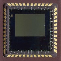
... Color Filter Array Mono RGB Bayer Pattern Packaging 48-pins LCC Cypress Semiconductor Corporation Document Number: 001-00371 Rev. *F LUPA-300 CMOS Image Sensor Figure 1. LUPA-300 CMOS Image Sensor Overview This document describes the interfacing and driving of the LUPA-300 image sensor. This VGA-resolution CMOS active pixel sensor features synchronous shutter and a maximal frame rate of 250 fps in full resolution ...
Page 2
... Ordering Information Marketing Part Number CYIL1SM0300AA-QDC CYIL1SM0300AA-QWC CYIL1SE0300AA-QDC CYIL1SM0300AA-WWC CYIL1SM0300-EVAL CYIL1SE0300-EVAL Specifications General Specifications Parameter Specifications Pixel Architecture 6 transistor pixel Pixel Size 9.9 µm x 9.9 µm Resolution 640 x 480 Pixel Rate 80 MHz Shutter Type Pipelined snapshot shutter Frame Rate 250 fps ...
Page 3
Spectral Response Curve 0.16 0.14 0.12 0.1 0.08 0.06 0.04 0.02 0 400 500 Photo-voltaic Response Curve 1.2 1 0.8 0.6 0.4 0.2 0 0.00E+00 1.00E+04 Document Number: 001-00371 Rev. *F Figure 2. Special Response of LUPA-300 600 700 Wavelength ...
Page 4
Features and General Specifications Table 1. General Specifications Feature Electronic shutter type Full snapshot shutter (integration during read out is possible) Windowing (ROI) Randomly programmable ROI read out. Implemented as scanning of lines/columns from an uploaded position Sub-sampling Sub sampling ...
Page 5
Table 3. Recommended Operating Conditions Symbol Parameter V Power supply of the analog readout circuitry. DDA V Digital power supply DDD V Power supply of the analog pixel array PIX V Power supply reset drivers RES V Power supply ...
Page 6
The 6-T pixel To obtain the global shutter feature combined with a high sensitivity and good Parasitic Light Sensitivity (PLS), the pixel architecture shown in Figure 5 is implemented. This pixel architecture is designed in a 9.9 x 9.9 m2 ...
Page 7
Windowing Windowing is achieved by the SPI interface. The starting point of the x- and y-address is uploadable, as well as the window size. The minimum step size in the x-direction is 8 pixels (only multiples of 8 can be ...
Page 8
This is why the default settings of the SPI are programmed to add an offset of 200 mV. This way the dark level goes from 1.3V to 1.5V and is the FPN information still converted by the ADC. To match ...
Page 9
ADC) to make sure the spread on the black level is still inside the range of the ADC after amplifi- cation. The result after amplification is the purple histogram Figure 9. Example of PGA Operation ...
Page 10
Biasing Table 10 summarizes the biasing signals required to drive this image sensor. For optimization reasons of the biasing of the column amplifiers with respect to power dissipation, several biasing resistors are required. This optimization results in an increase of ...
Page 11
Synchronous Shutter In a synchronous (snapshot or global) shutter light integration takes place on all pixels in parallel, although subsequent readout is sequential. Figure 10 shows the integration and read out sequence for the synchronous shutter. All pixels are light ...
Page 12
Table 12. Advantages and Disadvantages of Non Destructive Readout Advantages Low noise because true CDS. High sensitivity because the conversion capacitance is kept rather low. High dynamic range because the results includes signal for short and long ...
Page 13
Table 13. Internal Registers (continued) Address Bits 11 (1011) 11 (1100) 11 (1101) 11:0 14 (1110) 11:0 15 (1111) 8:0 Detailed Description of the Internal Registers The registers should ...
Page 14
Reverse_X (1bit) The readout direction in X can be reversed by setting this bit through the SPI. 1: Read direction is reversed (from right to left) 0: normal read direction (from left to right) - default Reverse_Y (1bit) The readout ...
Page 15
Bypass_mux (4 bits) These bits enable the possibility to bypass the digital multi- plexer. 0000: no bypass (default) PGA_SETTING <11:0> This register defines all parameters to set the PGA. The register consists of different "sub-registers" Gain_pga (4 ...
Page 16
The timing of the SPI register is explained in the timing diagram below 20 MHz SPI_CLK SPI_IN b<15> b<14> b<13> b<12> b<11> MSB---------------- Address bits------------- L SB MSB--------------------------------------------------------------------------------------- SPI_ENABLE SPI_IN (15:12): Address bits SPI_IN (11:0): Data bits When SPI_ENABLE is ...
Page 17
Integration frame I+1 Readout frame I FOT L1 ROT K1 Integration Timing Integration Timing in Mastermode In mastermode the integration time, the dual slope (DS) integration time, and triple slope (TS) integration time are set by the SPI settings. Figure ...
Page 18
The line counter starts with the value 1 immediately after the rising edge of RESET_N and after the end of the FOT. This means that the four integration timing registers must be uploaded with the desired number of lines plus ...
Page 19
Figure 17. Readout Time Smaller than Integration Time PIXEL RESET FOT FRAME_ VALID Readout Time Larger Than Integration Time In case the readout time is larger than then integration time, the RES_LENGTH register needs to be uploaded with a value ...
Page 20
RESET_N SPI SPI upload INT_TIME_1 INT_TIME_2 INT_TIME_3 RESET (internal ) DS RESET (internal ) TS RESET (internal ) PIXEL SAMPLE (internal ) FOT In case non destructive readout is used, the pulses on the input pins still need to be ...
Page 21
FRAME_VALID LINE_VALID The data at the output of the sensor is clocked on the rising edge of CLK. There is a delay of 3.2 ns between the rising edge of CLK and a change in DATA<9:0>. After this delay DATA<9:0> ...
Page 22
FOT INT_TIME1 Startup Timing On startup, VDDD should rise together with or before the other supplies. The rise of VDDD should be limited to 1V/100 μs to avoid activation of the on chip ESD protection circuitry. During the rise of ...
Page 23
Pinlist Table 15. Pinlist Pin No. Name Type 1 GND Ground ADC 2 DATA<5> Output 3 DATA<6> Output 4 DATA<7> Output 5 DATA<8> Output 6 DATA<9> Output 7 GND Ground Supply DDD 9 GND Ground ADC 10 ...
Page 24
Table 15. Pinlist (continued) Pin No. Name Type 31 INT_TIME_2 Digital I/O 32 INT_TIME_1 Digital I Supply DDD 34 GND Ground Supply DDA 36 GND Ground A 37 RESET_N Digital input 38 CLK Digital input ...
Page 25
Package Drawing Document Number: 001-00371 Rev. *F Figure 25. Package Drawing CYIL1SM0300AA Page [+] Feedback ...
Page 26
Package with Glass Die Specifications Pixel 0,0 Document Number: 001-00371 Rev ± 0.010m ± 0.13m m 8.6mm CYIL1SM0300AA ...
Page 27
Die in Package 31 Document Number: 001-00371 Rev. *F 7.1mm Optical center 48 1 CYIL1SM0300AA 19 7 Page [+] Feedback ...
Page 28
Bonding Diagram Document Number: 001-00371 Rev. *F CYIL1SM0300AA Page [+] Feedback ...
Page 29
Glass Lid A D263 glass is used as protection glass lid on top of the LUPA-300 monochrome and color sensors. characteristics of the D263 glass. Figure 26. Transmission Characteristics of the D263 Glass used as Protective Cover for the LUPA-300 ...
Page 30
Handling Precautions For proper handling and storage conditions, refer to the Cypress application note AN52561 at www.cypress.com. Limited Warranty Cypress Image Sensor Business Unit warrants that the image sensor products to be delivered hereunder if properly used and serviced, will ...
Page 31
... Cypress against all charges. Any Source Code (software and/or firmware) is owned by Cypress Semiconductor Corporation (Cypress) and is protected by and subject to worldwide patent protection (United States and foreign), United States copyright laws and international treaty provisions. Cypress hereby grants to licensee a personal, non-exclusive, non-transferable license to copy, use, modify, create derivative works of, and compile the Cypress Source Code and derivative works for the sole purpose of creating custom software and or firmware in support of licensee product to be used only in conjunction with a Cypress integrated circuit as specified in the applicable agreement ...