CYIL1SE0300-EVAL Cypress Semiconductor Corp, CYIL1SE0300-EVAL Datasheet - Page 15
CYIL1SE0300-EVAL
Manufacturer Part Number
CYIL1SE0300-EVAL
Description
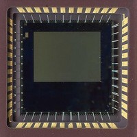
BOARD EVAL IMAGE SENSOR LUPA-300
Manufacturer
Cypress Semiconductor Corp
Datasheet
1.CYIL1SE0300-EVAL.pdf
(31 pages)
Specifications of CYIL1SE0300-EVAL
Sensor Type
CMOS Imaging, Color (RGB)
Sensing Range
VGA
Interface
SPI
Sensitivity
250 fps
Voltage - Supply
2.5 V ~ 3.3 V
Embedded
No
Utilized Ic / Part
LUPA-300
Lead Free Status / RoHS Status
Contains lead / RoHS non-compliant
Lead Free Status / RoHS Status
Lead free / RoHS Compliant, Contains lead / RoHS non-compliant


Bypass_mux (4 bits)
These bits enable the possibility to bypass the digital 4 to 1 multi-
plexer.
0000: no bypass (default)
PGA_SETTING <11:0>
This register defines all parameters to set the PGA. The register
consists of different "sub-registers"
Gain_pga (4 bits)
These bits set the gain of the PGA. The following
an overview of the different gain settings.
Table 14.
Unity_pga (1 bit)
This bit sets the PGA in unity amplification.
0: No unity amplification, gain settings apply
1: Unity gain amplification, gain setting are ignored (default)
Document Number: 001-00371 Rev. *F
0000
0001
0010
0011
0100
0101
0110
0111
1000
1001
1010
1011
1100
1101
1110
1111
GAIN_PGA<3:0>
1.32
1.56
1.85
2.18
2.58
3.05
3.59
4.22
4.9
5.84
6.84
8.02
9.38
11.2
13.12
15.38
Gain
Table 14
gives
Sel_uni (1 bit)
This bit selects whether or not the signal gets a 0.5 amplification
before the PGA.
0: amplification of 0.5 before PGA
1: Unity feed through (default)
Enable_analog_in (1 bit)
This bit enables/disables an analog input to the PGA.
0: analog input disabled (default)
1: analog input enabled
Enable_adc (4 bits)
These bits can separately enable/disable the different ADCs.
0000: No ADCs enabled
1111: All ADCs enabled (default)
0001: ADC 1 enabled
0010: ADC 2 enabled
Sel_calib_fast (1 bit)
Selects the fast/slow calibration of the ADC
0: slow calibration
1: fast calibration
2ADC Calibration Word <32:0>
The calibration word for the ADCs is distributed over three
registers (13, 14 and 15). These registers all have their default
value and changing this value is not recommended. The default
register values are:
calib_adc<11:0>: 101011011111
calib_adc<23:12>: 011011011011
calib_adc<32:24>: 000011011011
Data Interface (SPI)
The serial-3-wire interface (or Serial-to-Parallel Interface) uses a
serial input to shift the data in the register buffer. When the
complete data word is shifted into the register buffer the data
word is loaded into the internal register where it is decoded.
CYIL1SM0300AA
Page 15 of 31
[+] Feedback
Related parts for CYIL1SE0300-EVAL
Image
Part Number
Description
Manufacturer
Datasheet
Request
R

Part Number:
Description:
Manufacturer:
Cypress Semiconductor Corp
Datasheet:
Part Number:
Description:
Manufacturer:
Cypress Semiconductor Corp
Datasheet:
Part Number:
Description:
Manufacturer:
Cypress Semiconductor Corp
Datasheet:
Part Number:
Description:
Manufacturer:
Cypress Semiconductor Corp
Datasheet:
Part Number:
Description:
Manufacturer:
Cypress Semiconductor Corp
Datasheet: