CYIL1SE0300-EVAL Cypress Semiconductor Corp, CYIL1SE0300-EVAL Datasheet - Page 10
CYIL1SE0300-EVAL
Manufacturer Part Number
CYIL1SE0300-EVAL
Description
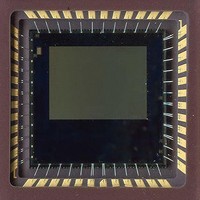
BOARD EVAL IMAGE SENSOR LUPA-300
Manufacturer
Cypress Semiconductor Corp
Datasheet
1.CYIL1SE0300-EVAL.pdf
(31 pages)
Specifications of CYIL1SE0300-EVAL
Sensor Type
CMOS Imaging, Color (RGB)
Sensing Range
VGA
Interface
SPI
Sensitivity
250 fps
Voltage - Supply
2.5 V ~ 3.3 V
Embedded
No
Utilized Ic / Part
LUPA-300
Lead Free Status / RoHS Status
Contains lead / RoHS non-compliant
Lead Free Status / RoHS Status
Lead free / RoHS Compliant, Contains lead / RoHS non-compliant


Biasing
Table 10
amplifiers with respect to power dissipation, several biasing resistors are required. This optimization results in an increase of signal
swing and dynamic range.
Table 10. Overview of Bias Signals
Digital Signals
Depending on the operation mode (master or slave), the pixel array of the image sensor requires different digital control signals. The
function of each of the signals is shown in
Table 11. Overview of Digital Signals
Document Number: 001-00371 Rev. *F
ADC_BIAS
PRECHARGE_BIAS
BIAS_PGA
BIAS_FAST
BIAS_SLOW
BIAS_COL
LINE_VALID
FRAME_VALID
INT_TIME_3
INT_TIME_2
INT_TIME_1
RESET_N
CLK
SPI_ENABLE
SPI_CLK
SPI_DATA
Note
5. Each biasing signal determines the operation of a corresponding module in the sense that it controls speed and dissipation.
Signal Name
Signal
summarizes the biasing signals required to drive this image sensor. For optimization reasons of the biasing of the column
[5]
Connect with 10 kΩ to V
Connect with 68 kΩ to V
GND
Biasing of amplifier stage. Connect with 110 kΩ to V
decouple with 100 nF to GND
Biasing of columns. Connect with 42 kΩ to V
100 nF to GND
Biasing of columns. Connect with 1.5 MΩ to V
100 nF to GND
Biasing of imager core. Connect with 500 kΩ to V
with 100 nF to GND
Digital output
Digital output
Digital I/O
Digital I/O
Digital I/O
Digital input
Digital input
Digital input
Digital input
Digital I/O
DRIVERS
I/O
A
A
Table
A
Indicates when valid data is at the outputs. Active high
Indicates when a valid frame is readout. Active high
In master mode: Output to indicate the triple slope integration time.
In slave mode: Input to control the triple slope integration time.
Active high
In master mode: Output to indicate the dual slope integration time.
In slave mode: Input to control the dual slope integration time.
Active high
In master mode: Output to indicate the integration time.
In slave mode: Input to control integration time.
Active high
Sequencer reset. Active low
Readout clock (80 MHz), sine or square clock
Enable of the SPI
Clock of the SPI. (Max. 20 MHz)
Data line of the SPI. Bidirectional pin
11:
ADC
PIX
and decouple with 100 nF to
Comment
and decouple with 100n to GND
A
DDA
DDA
and decouple with
and decouple with
DDA
DDA
and decouple
and
Comments
ADC
Pixel array precharge
Column amplifiers
Column amplifiers
Column amplifiers
Related Module
CYIL1SM0300AA
ADC
PGA
Page 10 of 31
DC-Level‘
693 mV
567 mV
650 mV
750 mV
450 mV
508 mV
[+] Feedback
Related parts for CYIL1SE0300-EVAL
Image
Part Number
Description
Manufacturer
Datasheet
Request
R

Part Number:
Description:
Manufacturer:
Cypress Semiconductor Corp
Datasheet:
Part Number:
Description:
Manufacturer:
Cypress Semiconductor Corp
Datasheet:
Part Number:
Description:
Manufacturer:
Cypress Semiconductor Corp
Datasheet:
Part Number:
Description:
Manufacturer:
Cypress Semiconductor Corp
Datasheet:
Part Number:
Description:
Manufacturer:
Cypress Semiconductor Corp
Datasheet: