CYIL1SE0300-EVAL Cypress Semiconductor Corp, CYIL1SE0300-EVAL Datasheet - Page 19
CYIL1SE0300-EVAL
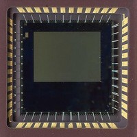
Manufacturer Part Number
CYIL1SE0300-EVAL
Description
BOARD EVAL IMAGE SENSOR LUPA-300
Manufacturer
Cypress Semiconductor Corp
Datasheet
1.CYIL1SE0300-EVAL.pdf
(31 pages)
Specifications of CYIL1SE0300-EVAL
Sensor Type
CMOS Imaging, Color (RGB)
Sensing Range
VGA
Interface
SPI
Sensitivity
250 fps
Voltage - Supply
2.5 V ~ 3.3 V
Embedded
No
Utilized Ic / Part
LUPA-300
Lead Free Status / RoHS Status
Contains lead / RoHS non-compliant
Lead Free Status / RoHS Status
Lead free / RoHS Compliant, Contains lead / RoHS non-compliant


Readout Time Larger Than Integration Time
In case the readout time is larger than then integration time, the
RES_LENGTH register needs to be uploaded with a value larger
than two to compensate for the larger readout time. The
Integration Timing in Slave Mode
In slave mode, the registers RES_LENGTH, DS_TIMER,
TS_TIMER, and FT_TIMER are ignored. The integration timing
is now controlled by the pins INT_TIME_1, INT_TIME_2 and
INT_TIME_3, which are now active low input pins.
The relationship between the input pins and the integration
timing is illustrated in
IN_TIME_1 is low (active) and INT_TIME_2 and INT_TIME_3
Document Number: 001-00371 Rev. *F
FRAME_ VALID
FRAME_ VALID
RESET
PIXEL
Figure
RESET
PIXEL
19. The pixel is reset as soon as
FOT
Figure 17. Readout Time Smaller than Integration Time
Figure 18. Readout Time Larger than Integration Time
FOT
Readout
FT_TIMER
Readout
Total Integration Time
FT_TIMER
Integration Time
FT_TIMER register must be set to the desired window size (in
Y). Only the RES_LENGTH register needs to be changed during
operation.
are high. The integration starts when INT_TIME_1 becomes high
again and during this integration additional (lower) reset can be
given by activating INT_TIME_2 and INT_TIME_3 separately. At
the end of the desired integration time the frame transfer starts
by making all 3 INT_TIME pins active low simultaneously. There
is always a small delay between the applied external signals and
the actual internally generated pulses. These delays are also
shown in
Figure
Figure 18
FOT
FOT
19.
shows this example.
CYIL1SM0300AA
Page 19 of 31
[+] Feedback
Related parts for CYIL1SE0300-EVAL
Image
Part Number
Description
Manufacturer
Datasheet
Request
R

Part Number:
Description:
Manufacturer:
Cypress Semiconductor Corp
Datasheet:
Part Number:
Description:
Manufacturer:
Cypress Semiconductor Corp
Datasheet:
Part Number:
Description:
Manufacturer:
Cypress Semiconductor Corp
Datasheet:
Part Number:
Description:
Manufacturer:
Cypress Semiconductor Corp
Datasheet:
Part Number:
Description:
Manufacturer:
Cypress Semiconductor Corp
Datasheet: