CYIL1SE0300-EVAL Cypress Semiconductor Corp, CYIL1SE0300-EVAL Datasheet - Page 16
CYIL1SE0300-EVAL
Manufacturer Part Number
CYIL1SE0300-EVAL
Description
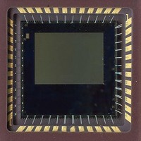
BOARD EVAL IMAGE SENSOR LUPA-300
Manufacturer
Cypress Semiconductor Corp
Datasheet
1.CYIL1SE0300-EVAL.pdf
(31 pages)
Specifications of CYIL1SE0300-EVAL
Sensor Type
CMOS Imaging, Color (RGB)
Sensing Range
VGA
Interface
SPI
Sensitivity
250 fps
Voltage - Supply
2.5 V ~ 3.3 V
Embedded
No
Utilized Ic / Part
LUPA-300
Lead Free Status / RoHS Status
Contains lead / RoHS non-compliant
Lead Free Status / RoHS Status
Lead free / RoHS Compliant, Contains lead / RoHS non-compliant


The timing of the SPI register is explained in the timing diagram below
SPI_IN (15:12): Address bits
SPI_IN (11:0): Data bits
When SPI_ENABLE is asserted the parallel data is loaded into
the internal registers of the LUPA300. The frequency of SPI_CLK
is 20 MHz or lower. The SPI bits have a default value that allows
the sensor to be read out at full resolution without uploading the
SPI bits.
Timing and Readout of the Image Sensor
The timing of the sensor consists of two parts. The first part is
related with the integration time and the control of the pixel. The
second part is related to the readout of the image sensor.
Integration and readout can be in parallel. In this case, the
integration time of frame I is ongoing during readout of frame I-1.
Figure 14
The readout of every frame starts with a Frame Overhead Time
(FOT) during which the analog value on the pixel diode is trans-
Document Number: 001-00371 Rev. *F
SPI_ENABLE
SPI_CLK
SPI_IN
shows this parallel timing structure.
b<15>
MSB---------------- Address bits------------- L SB
20 MHz
b<14>
b<13>
b<12>
b<11>
MSB---------------------------------------------------------------------------------------
b<10>
b<9>
Figure 13. Timing of the SPI
Figure 12. SPI Schematic
b<8>
b<7>
Upload
b<6>
ferred to the pixel memory element. After this FOT, the sensor is
read out line per line. The readout of every line starts with a Row
Overhead Time (ROT) during which the pixel value is put on the
column lines. Then the pixels are selected in groups of 4. So in
total 160 kernels of 4 pixels are read out. The internal timing is
generated by the sequencer. The sequencer can operate in 2
modes: master mode and slave mode. In master mode all the
internal timing is controlled by the sequencer, based on the SPI
settings. In slave mode the integration timing is directly
controlled over three pins, the readout timing is still controlled by
the sequencer. The selection between master and slave mode is
done by the MASTERMODE register of the SPI. The sequencer
is clocked on the core clock; this is the same clock as the ADCs.
The core clock is the input clock divided by 4.
Data bits--------------------------------------------------------------------------------
b<5>
b<4>
b<3>
b<2>
b<1>
b<0>
LSB
CYIL1SM0300AA
dummy
b<15>
b<14>
Page 16 of 31
b<13>
[+] Feedback
Related parts for CYIL1SE0300-EVAL
Image
Part Number
Description
Manufacturer
Datasheet
Request
R

Part Number:
Description:
Manufacturer:
Cypress Semiconductor Corp
Datasheet:
Part Number:
Description:
Manufacturer:
Cypress Semiconductor Corp
Datasheet:
Part Number:
Description:
Manufacturer:
Cypress Semiconductor Corp
Datasheet:
Part Number:
Description:
Manufacturer:
Cypress Semiconductor Corp
Datasheet:
Part Number:
Description:
Manufacturer:
Cypress Semiconductor Corp
Datasheet: