CYIL1SE0300-EVAL Cypress Semiconductor Corp, CYIL1SE0300-EVAL Datasheet - Page 7
CYIL1SE0300-EVAL
Manufacturer Part Number
CYIL1SE0300-EVAL
Description
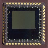
BOARD EVAL IMAGE SENSOR LUPA-300
Manufacturer
Cypress Semiconductor Corp
Datasheet
1.CYIL1SE0300-EVAL.pdf
(31 pages)
Specifications of CYIL1SE0300-EVAL
Sensor Type
CMOS Imaging, Color (RGB)
Sensing Range
VGA
Interface
SPI
Sensitivity
250 fps
Voltage - Supply
2.5 V ~ 3.3 V
Embedded
No
Utilized Ic / Part
LUPA-300
Lead Free Status / RoHS Status
Contains lead / RoHS non-compliant
Lead Free Status / RoHS Status
Lead free / RoHS Compliant, Contains lead / RoHS non-compliant


Windowing
Windowing is achieved by the SPI interface. The starting point of
the x- and y-address is uploadable, as well as the window size.
The minimum step size in the x-direction is 8 pixels (only
multiples of 8 can be chosen as start/stop addresses). The
Table 5. Typical Frame Rates for 80 MHz Clock and GRAN<1:0>=10
Analog to Digital Converter
The sensor has four 10-bit pipelined ADC on board. The ADCs
are nominally operating at 20 Msamples/s. The input range of the
ADC is between 0.75 and 1.75V. The analog input signal is
sampled at 2.1 ns delay from the rising edge of the ADC clock.
Table 6. ADC Parameters
Document Number: 001-00371 Rev. *F
Data rate
Input range
Quantization
DNL
INL
Image resolution (X * Y)
ADC_OUT
CLK_ADC
ADC_IN
Parameter
<9:0>
640 x 480
640 x 240
256 x 256
20 Msamples/s
0.75V - 1.75 V
10 bit
Typ. < 0.3 LSB
Typ. < 0.7 LSB
D1
Frame Rate (fps)
50ns
Specification
D2
247.5
488.3
1076
5.5 clock cycles
DUMMY
D3
Figure 6. ADC Timing
D4
Frame Readout (us)
minimum step size in the y-direction is 1 line (every line can be
addressed) in normal mode and 2 lines in sub sampling mode.
The window size in the x-direction is uploadable in register
NB_OF_PIX. The window size in the y-direction is determined by
the register FT_TIMER
The digital output data appears at the output at 5.5 cycles later.
This is at the 6th falling edge succeeding the sample moment.
The data is delayed by 3.7 ns with respect to this falling edge.
This is illustrated in
Programmable Gain Amplifiers
The programmable gain amplifiers have two functions:
■
■
Offset Regulation
The purpose of offset regulation is to bring the signal in the input
range of the ADC.
After the column amplifiers, the signal from the pixels has a
range from 0.1V (bright) to 1.3V (black). The input range of the
ADC is from 0.75V to 1.75V. The amount of offset added is
controlled
VOFFSET<7:0>. The formula to add offset is:
Voutput = Vsignal + (Voffset - Vblack)
Note that the FPN (fixed pattern noise) of the sensor causes a
spread of about 100 mV on the dark level. To allow FPN
correction during post processing of the image, this spread on
the dark level needs to be covered by the input range of the ADC.
Adding an offset to the signal to fit it into the range of the ADC.
This is controlled by the VBLACK and VOFFSET SPI settings.
Amplifying the signal after the offset is added.
D5
4038
2048
929
3.7ns
by
D6
D1
two
Figure
D7
SPI
6.
D2
settings:
D8
CYIL1SM0300AA
Sub sampling
D3
Windowing
Comment
VBLACK<7:0>
D4
Page 7 of 31
and
[+] Feedback
Related parts for CYIL1SE0300-EVAL
Image
Part Number
Description
Manufacturer
Datasheet
Request
R

Part Number:
Description:
Manufacturer:
Cypress Semiconductor Corp
Datasheet:
Part Number:
Description:
Manufacturer:
Cypress Semiconductor Corp
Datasheet:
Part Number:
Description:
Manufacturer:
Cypress Semiconductor Corp
Datasheet:
Part Number:
Description:
Manufacturer:
Cypress Semiconductor Corp
Datasheet:
Part Number:
Description:
Manufacturer:
Cypress Semiconductor Corp
Datasheet: