CYIL1SE0300-EVAL Cypress Semiconductor Corp, CYIL1SE0300-EVAL Datasheet - Page 8
CYIL1SE0300-EVAL
Manufacturer Part Number
CYIL1SE0300-EVAL
Description
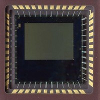
BOARD EVAL IMAGE SENSOR LUPA-300
Manufacturer
Cypress Semiconductor Corp
Datasheet
1.CYIL1SE0300-EVAL.pdf
(31 pages)
Specifications of CYIL1SE0300-EVAL
Sensor Type
CMOS Imaging, Color (RGB)
Sensing Range
VGA
Interface
SPI
Sensitivity
250 fps
Voltage - Supply
2.5 V ~ 3.3 V
Embedded
No
Utilized Ic / Part
LUPA-300
Lead Free Status / RoHS Status
Contains lead / RoHS non-compliant
Lead Free Status / RoHS Status
Lead free / RoHS Compliant, Contains lead / RoHS non-compliant


This is why the default settings of the SPI are programmed to
add an offset of 200 mV. This way the dark level goes from 1.3V
to 1.5V and is the FPN information still converted by the ADC. To
match the ADC range, it is recommended to program an offset
of 340 mV. To program this offset, the Voffset and Vblack
registers can be used.
offset regulation with an example. The blue histogram is the
histogram of the image taken after the column amplifiers.
Consider as an example that the device has a black level of
1.45V and a swing of 100 mV. With this swing, it fits in the input
range of the ADC, but a large part of the range of the ADC is not
used in this case. For this reason an offset is added first, to align
the black level with the input range of the ADC. In the first step,
an offset of 200 mV is added with the default settings of VBLACK
and VOFFSET. This results in the red histogram with a average
black level of 1.65V. This means that the spread on the black
level falls completely inside the range of the ADC. In a second
step, the signal is amplified to use the full range of the ADC.
Figure 7. Offset Regulation
Programmable Gain
The amplification inside the PGA is controlled by three SPI
settings:
The PGA gain selection: 16 gain steps are selectable by means
of the GAIN_PGA<3:0> register. Selection word 0000
corresponds with gain 1.32 and selection word 1111 corresponds
with gain 15.5.
The unity gain selection of the PGA is done by the UNITY_PGA
setting. If this bit is high, the GAIN_PGA settings are ignored.
The SEL_UNI setting is used to have more gain steps. If this bit
is low, the signal is divided by two before entering the PGA.
GAIN_PGA and UNITY_PGA settings are applied afterwards. If
the SEL_UNI bit is high, there is a unity feed through to the PGA.
This allows having a total gain range of 0.5 to 16 in 32 steps.
Document Number: 001-00371 Rev. *F
Table 7
gives the 16 gain settings
Figure 7
1.45V
illustrates the operation of the
1.65V
1.75V
VADC_HIGH
Volts
Table 7. Gain Settings
The amplification in the PGA is done around a pivoting point, set
by Vcal as illustrated in
to apply the Vcal voltage through an on chip DAC
Figure 8. Effect on Histogram of PGA (gain=4)
(Vcal is the green line)
Figure 9
Regulation. The blue histogram is the histogram of the image
after the column amplifiers. With offset regulation an offset of 200
mV is added to bring the signal in range of the ADC. The black
level of 1.45V is shifted to 1.65V.
The red and blue histograms have a swing of 100 mV. This
means the input range of the ADC is not completely used. By
amplifying the signal with a factor 10 by the PGA, the full range
of the ADC can be used. In this example, Vcal is set at 1.75V (the
GAIN_PGA<3.0>
continues on the example in the section,
0000
0001
0010
0011
0100
0101
0110
1000
1001
1010
1011
1100
1101
0111
1110
1111
Vcal
Figure
8. The VCAL<7:0> setting is used
CYIL1SM0300AA
13.12
15.38
Gain
1.32
1.56
1.85
2.18
2.58
3.05
3.59
4.22
5.84
6.84
8.02
9.38
11.2
4.9
Page 8 of 31
Volts
Offset
[+] Feedback
Related parts for CYIL1SE0300-EVAL
Image
Part Number
Description
Manufacturer
Datasheet
Request
R

Part Number:
Description:
Manufacturer:
Cypress Semiconductor Corp
Datasheet:
Part Number:
Description:
Manufacturer:
Cypress Semiconductor Corp
Datasheet:
Part Number:
Description:
Manufacturer:
Cypress Semiconductor Corp
Datasheet:
Part Number:
Description:
Manufacturer:
Cypress Semiconductor Corp
Datasheet:
Part Number:
Description:
Manufacturer:
Cypress Semiconductor Corp
Datasheet: