CYIL1SE0300-EVAL Cypress Semiconductor Corp, CYIL1SE0300-EVAL Datasheet - Page 5
CYIL1SE0300-EVAL
Manufacturer Part Number
CYIL1SE0300-EVAL
Description
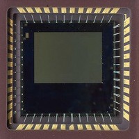
BOARD EVAL IMAGE SENSOR LUPA-300
Manufacturer
Cypress Semiconductor Corp
Datasheet
1.CYIL1SE0300-EVAL.pdf
(31 pages)
Specifications of CYIL1SE0300-EVAL
Sensor Type
CMOS Imaging, Color (RGB)
Sensing Range
VGA
Interface
SPI
Sensitivity
250 fps
Voltage - Supply
2.5 V ~ 3.3 V
Embedded
No
Utilized Ic / Part
LUPA-300
Lead Free Status / RoHS Status
Contains lead / RoHS non-compliant
Lead Free Status / RoHS Status
Lead free / RoHS Compliant, Contains lead / RoHS non-compliant


:
Table 3. Recommended Operating Conditions
Sensor Architecture
The floor plan of the architecture is shown in
core consists of a pixel array, an X- and Y-addressing register,
pixel array drivers, and column amplifiers. The image sensor of
640 x 480 pixels is read out in progressive scan.
The architecture allows programmable addressing in the
x-direction in steps of 8 pixels and in the y-direction in steps of 1
Document Number: 001-00371 Rev. *F
Notes
V
V
V
V
V
V
T
A
2. All parameters are characterized for DC conditions after thermal equilibrium has been established.
3. Unused inputs must always be tied to an appropriate logic level, for example, either VDD or GND.
4. This device contains circuitry to protect the inputs against damage due to high static voltages or electric fields; however, it is recommended that normal precautions
A
DDA
DDD
PIX
RES
MEM_H
ADC
L
be taken to avoid application of any voltages higher than the maximum rated voltages to this high impedance circuit.
Symbol
Power supply of the analog readout circuitry.
Digital power supply
Power supply of the analog pixel array
Power supply reset drivers
Power supply of the pixels memory element (high level)
Power supply of the on-chip ADCs
Commercial operating temperature.
Maximum lens angle
Parameter
PGA + ADC
Figure
Figure 4. Floor Plan of the Sensor
[2,3,4]
4. The image
PGA + ADC
Column amplifiers
On chip drivers
X-shift register
10 bit output
Pixel array
640 x 480
pixel. The starting point of the address is uploadable by means
of the Serial Parallel Interface (SPI).
The PGAs amplify the signal from the column and add an offset
so the signal fits in the input range of the ADC. The four ADCs
then convert the signal to the digital domain. Pixels are selected
in a 4 * 1 kernel. Every ADC samples the signal from one of the
4 selected pixels. Sampling frequency is 20 MHz. The digital
outputs of the four ADCs are multiplexed to one output bus
operating at 80 MHz.
Mux
PGA + ADC
Min
–40
2.5
2.5
Sequencer
PGA + ADC
Typ
2.5
2.5
2.5
3.3
3.3
2.5
30
CYIL1SM0300AA
Max
3.5
3.5
70
25
Unit
Page 5 of 31
°C
V
V
V
V
V
V
°
[+] Feedback
Related parts for CYIL1SE0300-EVAL
Image
Part Number
Description
Manufacturer
Datasheet
Request
R

Part Number:
Description:
Manufacturer:
Cypress Semiconductor Corp
Datasheet:
Part Number:
Description:
Manufacturer:
Cypress Semiconductor Corp
Datasheet:
Part Number:
Description:
Manufacturer:
Cypress Semiconductor Corp
Datasheet:
Part Number:
Description:
Manufacturer:
Cypress Semiconductor Corp
Datasheet:
Part Number:
Description:
Manufacturer:
Cypress Semiconductor Corp
Datasheet: