CYIL1SE0300-EVAL Cypress Semiconductor Corp, CYIL1SE0300-EVAL Datasheet - Page 12
CYIL1SE0300-EVAL
Manufacturer Part Number
CYIL1SE0300-EVAL
Description
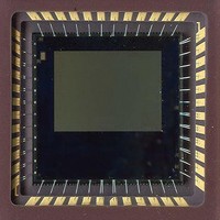
BOARD EVAL IMAGE SENSOR LUPA-300
Manufacturer
Cypress Semiconductor Corp
Datasheet
1.CYIL1SE0300-EVAL.pdf
(31 pages)
Specifications of CYIL1SE0300-EVAL
Sensor Type
CMOS Imaging, Color (RGB)
Sensing Range
VGA
Interface
SPI
Sensitivity
250 fps
Voltage - Supply
2.5 V ~ 3.3 V
Embedded
No
Utilized Ic / Part
LUPA-300
Lead Free Status / RoHS Status
Contains lead / RoHS non-compliant
Lead Free Status / RoHS Status
Lead free / RoHS Compliant, Contains lead / RoHS non-compliant


Table 12. Advantages and Disadvantages of Non Destructive Readout
Sequencer
The sequencer generates the complete internal timing of the
pixel array and the readout. The timing can be controlled by the
user through the SPI register settings. The sequencer operates
Table 13. Internal Registers
Document Number: 001-00371 Rev. *F
Low noise because it is a true CDS.
High sensitivity because the conversion capacitance is kept
rather low.
High dynamic range because the results includes signal for
short and long integrations times.
0 (0000)
1 (0001)
2 (0010)
3 (0011)
4 (0100)
5 (0101)
6 (0110)
7(0111)
8 (1000)
9 (1001)
10 (1010)
Address
Advantages
10:0
1
1
2
1
1
1
1
1
1
1
7:0
8:0
7:0
11:0
11:0
11:0
11:0
7:0
7:0
7:0
Bits
START_X
START_Y
VBLACK
VOFFSET
SEQUENCER
mastermode
ss
gran
enable_analog_out
calib_line
res2_en
res3_en
reverse_x
reverse_y
Ndr
NB_PIX
RES1_LENGTH
RES2_TIMER
RES3_TIMER
FT_TIMER
VCAL
Name
System memory required to record the reset level and the interme-
diate samples.
Requires multiples readings of each pixel, thus higher data
throughput.
Requires system level digital calculations.
on the same clock as the ADCs. This is a division by 4 of the input
clock.
Table 13
description. In the next section, the registers are explained in
more detail.
shows a list of the internal registers with a short
Default <10:0>: 00000101001
1: master mode; 0: slave mode
1: ss in y; 0: no subsampling
clock granularity
1: enabled; 0: disabled
1: line calibration; 0 frame calibration
1: enable DS; 0: Disable DS
1: enable TS; 0: Disable TS
1: readout in reverse x direction
0: readout in normal x direction
1: readout in reverse y direction
0: readout in normal y direction
1: enable non destructive readout
0: disable non destructive readout
Start pointer X readout
Default <7:0>: 00000000
Start pointer Y readout
Default <8:0>: 000000000
Number of kernels to read out (4 pixel kernel)
Default <7:0>: 10100000
Length of reset pulse (in number of lines)
Default <11:0>: 000000000010
Position of reset DS pulse in number of lines
Default <11:0>: 000000000000
Position of reset TS pulse in number of lines
Default <11:0>: 000000000000
Position of frame transfer in number of lines
Default <11:0>: 000111100001
DAC input for vcal
Default <7:0>: 01001010
DAC input for vblack
Default <7:0>: 01101011
DAC input for voffset
Default <7:0>: 01010101
Disadvantages
Description
CYIL1SM0300AA
Page 12 of 31
[+] Feedback
Related parts for CYIL1SE0300-EVAL
Image
Part Number
Description
Manufacturer
Datasheet
Request
R

Part Number:
Description:
Manufacturer:
Cypress Semiconductor Corp
Datasheet:
Part Number:
Description:
Manufacturer:
Cypress Semiconductor Corp
Datasheet:
Part Number:
Description:
Manufacturer:
Cypress Semiconductor Corp
Datasheet:
Part Number:
Description:
Manufacturer:
Cypress Semiconductor Corp
Datasheet:
Part Number:
Description:
Manufacturer:
Cypress Semiconductor Corp
Datasheet: