DK-DEV-2AGX260N Altera, DK-DEV-2AGX260N Datasheet
DK-DEV-2AGX260N
Specifications of DK-DEV-2AGX260N
Available stocks


Related parts for DK-DEV-2AGX260N


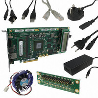
DK-DEV-2AGX260N Summary of contents
Page 1
... Arria II GX FPGA Development Board, 6G Edition 101 Innovation Drive San Jose, CA 95134 www.altera.com Reference Manual Document Version: Document Date: July 2010 1.0 ...
Page 2
... Altera warrants performance of its semiconductor products to current specifications in accordance with Altera's standard warranty, but reserves the right to make changes to any products and services at any time without notice. Altera assumes no responsibility or liability arising out of the application or use of any information, product, or service described herein except as expressly agreed to in writing by Altera Corporation ...
Page 3
... High-Speed Mezzanine Cards . . . . . . . . . . . . . . . . . . . . . . . . . . . . . . . . . . . . . . . . . . . . . . . . . . . . . . . . . 2–31 Memory . . . . . . . . . . . . . . . . . . . . . . . . . . . . . . . . . . . . . . . . . . . . . . . . . . . . . . . . . . . . . . . . . . . . . . . . . . . . . . . 2–38 DDR3 . . . . . . . . . . . . . . . . . . . . . . . . . . . . . . . . . . . . . . . . . . . . . . . . . . . . . . . . . . . . . . . . . . . . . . . . . . . . . . 2–38 DDR2 SODIMM . . . . . . . . . . . . . . . . . . . . . . . . . . . . . . . . . . . . . . . . . . . . . . . . . . . . . . . . . . . . . . . . . . . . . 2–40 SSRAM . . . . . . . . . . . . . . . . . . . . . . . . . . . . . . . . . . . . . . . . . . . . . . . . . . . . . . . . . . . . . . . . . . . . . . . . . . . . . 2–44 Flash . . . . . . . . . . . . . . . . . . . . . . . . . . . . . . . . . . . . . . . . . . . . . . . . . . . . . . . . . . . . . . . . . . . . . . . . . . . . . . . 2–47 Power Supply . . . . . . . . . . . . . . . . . . . . . . . . . . . . . . . . . . . . . . . . . . . . . . . . . . . . . . . . . . . . . . . . . . . . . . . . . . 2–49 Power Distribution System . . . . . . . . . . . . . . . . . . . . . . . . . . . . . . . . . . . . . . . . . . . . . . . . . . . . . . . . . . . . 2–49 Power Measurement . . . . . . . . . . . . . . . . . . . . . . . . . . . . . . . . . . . . . . . . . . . . . . . . . . . . . . . . . . . . . . . . . 2–51 Statement of China-RoHS Compliance . . . . . . . . . . . . . . . . . . . . . . . . . . . . . . . . . . . . . . . . . . . . . . . . . . . . 2–52 © July 2010 Altera Corporation Arria II GX FPGA Development Board, 6G Edition Reference Manual ry Contents ...
Page 4
... Additional Information Revision History . . . . . . . . . . . . . . . . . . . . . . . . . . . . . . . . . . . . . . . . . . . . . . . . . . . . . . . . . . . . . . . . . . . . . Info–1 How to Contact Altera . . . . . . . . . . . . . . . . . . . . . . . . . . . . . . . . . . . . . . . . . . . . . . . . . . . . . . . . . . . . . . . . Info–1 Typographic Conventions . . . . . . . . . . . . . . . . . . . . . . . . . . . . . . . . . . . . . . . . . . . . . . . . . . . . . . . . . . . . . Info–2 Arria II GX FPGA Development Board, 6G Edition Reference Manual © July 2010 Altera Corporation ary ...
Page 5
... The board provides a wide range of peripherals and memory interfaces to facilitate the development of the Arria II GX FPGA designs. Two high-speed mezzanine card (HSMC) connector is available to add additional functionality via a variety of HSMCs available from Altera f To see a list of the latest HSMCs available or to download a copy of the HSMC specification, refer to the website ...
Page 6
... Programmable oscillator with a default frequency of 100-MHz ■ SMA connectors for external LVPECL clock input ■ SMA connector for clock output ■ Arria II GX FPGA Development Board, 6G Edition Reference Manual TM for use with the Quartus ® II Programmer Chapter 1: Overview Board Component Blocks © July 2010 Altera Corporation ...
Page 7
... PCI Express edge connector power ■ On-board power measurement circuitry ■ Mechanical ■ PCI Express full-length standard-height (8.48” x 4.376”) ■ PCI Express chassis or bench-top operation ■ © July 2010 Altera Corporation Arria II GX FPGA Development Board, 6G Edition Reference Manual 1–3 ...
Page 8
... EP2AGX260FF35 64 MB Flash CPLD x8 Edge Chapter 1: Overview Development Board Block Diagram Z Z USB Embedded 2.0 Blaster JTAG Chain x50 128 MB DDR3 (x16) x11 2x16 LCD x3 Push-button Switches x4 DIP Switch x4 LEDs x26 ADDR x32 DATA 2 MB SSRAM © July 2010 Altera Corporation ...
Page 9
... Board Overview This section provides an overview of the Arria II GX FPGA development board, 6G Edition, including an annotated board image and component descriptions. provides an overview of the development board features. © July 2010 Altera Corporation 2. Board Components Figure 2–1 illustrates major component locations and Arria II GX FPGA Development Kit, 6G Edition User Arria II GX FPGA Development Board, 6G Edition Reference Manual Table 2– ...
Page 10
... Configuration LEDs (D11-D16) Load Image (PB5), Image Select Push-button Switch (PB6) DDR3 x16 (U13) Power Switch (SW1) DC Input Jack (J4) SSRAM x36 Memory (U22) Character LCD (J3) Flash x16 Memory (U23) Fan Power (J13) Board Settings DIP Switch (SW4) Description © July 2010 Altera Corporation ...
Page 11
... Image select push-button switch PB5 Load image push-button switch © July 2010 Altera Corporation Description Illuminates to show the LED sequence that determines which flash memory image loads to the FPGA when LOAD IMAGE is pressed. Shows the connection speed as well as transmit or receive activity. ...
Page 12
... USB interface for programming the FPGA through embedded USB-Blaster JTAG via a type-B USB cable. RJ-45 connector which provides a 10/100/1000 Ethernet connection via a Marvell 88E1111 PHY and the FPGA-based Altera Triple Speed Ethernet MegaCore function in RGMII mode. Connector which interfaces to the provided 16 character × 2 line LCD module along with two standoffs at MTH7 and MTH8 ...
Page 13
... I/O count for the EP2AGX125 and EP2AGX260 device in the 1152-pin FBGA package. Figure 2–2. EP2AGX125 and EP2AGX260 Device I/O Bank Diagram Bank 8C Bank 3C © July 2010 Altera Corporation Total RAM 18-bit × 18-bit Kbits Multipliers PLLs ...
Page 14
... The HSMC port B is populated when the board uses an EP2AGX260 device. To support the HSMC port B, there are two additional LEDs and a REFCLK in quadrant 3. MAX II CPLD EPM2210 System Controller The board utilizes the EPM2210 System Controller, an Altera MAX II CPLD, for the following purposes: ■ ...
Page 15
... July 2010 Altera Corporation JTAG Control SLD-HUB Decoder Virtual-JTAG Power Calculations EPM2210 EP2AGX125 Pin Number Pin Number K14 — DIP - clock oscillator enable P2 — ...
Page 16
... FPGA configuration data A5 M4 FPGA configuration data B6 K2 FPGA configuration data H4 L25 FPGA configuration clock J2 AC26 FPGA configuration active H3 AD28 FPGA configuration ready A2 M21 FSM bus address Chapter 2: Board Components MAX II CPLD EPM2210 System Controller Description © July 2010 Altera Corporation ...
Page 17
... July 2010 Altera Corporation EPM2210 EP2AGX125 Pin Number Pin Number D9 J3 FSM bus address B16 C24 FSM bus address C15 E25 FSM bus address D16 ...
Page 18
... M11 C15 FSM bus Max2 byte enable 0 M10 H16 FSM bus Max2 byte enable 1 N12 D14 FSM bus Max2 byte enable 2 P12 A9 FSM bus Max2 byte enable 3 Chapter 2: Board Components MAX II CPLD EPM2210 System Controller Description © July 2010 Altera Corporation ...
Page 19
... FPGA Programming over Embedded USB-Blaster The USB-Blaster is implemented using a USB Type-B connector (J6), a FTDI USB 2.0 PHY device (U15), and an Altera MAX II CPLD (U32). This allows the configuration of the FPGA using a USB cable directly connected between the USB port on the board (J6) and a USB port running the Quartus II software ...
Page 20
... Configuration, Status, and Setup Elements ALWAYS EP2AGX125 ENABLED FPGA (in chain) JTAG Slave MAX II CPLD EPM2210 Flash System Memory Controller JTAG Slave Installed HSMC HSMC Port A Card Installed HSMC HSMC Port B Card PCI Express PCI Express Edge Motherboard Connector © July 2010 Altera Corporation ...
Page 21
... The development board implements the Altera PFL megafunction for flash memory programming. The PFL megafunction is a block of logic that is programmed into an Altera programmable logic device (FPGA or CPLD). The PFL functions as a utility for writing to a compatible flash memory device. This ...
Page 22
... MHz CONF_DONE_LED MSEL [3:0] 2.5 V Chapter 2: Board Components Configuration, Status, and Setup Elements 10 kΩ INIT_DONE MSEL3 nSTATUS MSEL2 nCONFIG MSEL1 CONF_DONE MSEL0 nCE FPP Port DATA [7:0] Flash Interface DCLK 10 kΩ © July 2010 Altera Corporation 10 kΩ ...
Page 23
... Otherwise, the user hardware page 1 is loaded. Pressing the load image push-button switch (PB5) loads the FPGA with a hardware page based on which CONFIG[2:0] LED (D11, D12, D13) is illuminated. hardware page that loads when the load image push-button switch (PB5) is pressed. © July 2010 Altera Corporation Name Size (Kbyte) 32 ...
Page 24
... Marvell 88E1111 PHY. Green LED. Illuminates to indicate Ethernet PHY receive activity. Driven by the Marvell 88E1111 PHY. Chapter 2: Board Components Configuration, Status, and Setup Elements (1) (2) IMAGE2 Design OFF Factory hardware OFF User hardware 1 ON User hardware 2 Guide. © July 2010 Altera Corporation ...
Page 25
... Reserved MAX_DIP0 2 Reserved MAX_DIP1 © July 2010 Altera Corporation Description Green LED. Illuminates to indicate Ethernet linked at 10 Mbps connection speed. Driven by the Marvell 88E1111 PHY. Green LED. Illuminates to indicate Ethernet linked at 100 Mbps connection speed. Driven by the Marvell 88E1111 PHY. Green LED. Illuminates to indicate Ethernet linked at 1000 Mbps connection speed. ...
Page 26
... ON : Bypass HSMA OFF : HSMA in-chain ON : Bypass HSMB OFF : HSMB in-chain ON : Bypass PCI Express OFF : Reserved (disables JTAG chain, do not use) Chapter 2: Board Components Configuration, Status, and Setup Elements Default OFF OFF ON OFF ON ON Manufacturer Website www.hchtwn.com.tw Default © July 2010 Altera Corporation ...
Page 27
... The image select push-button switch, factory (IMAGE SEL) (PB6), toggles the LED_CONFIG_LED[2:0] sequence. Refer to LED_CONFIG_LED[2:0] sequence definitions. The MAX II reset push-button switch, MAX_RESETn (PB4), resets the MAX II CPLD EPM2210 System Controller. © July 2010 Altera Corporation Manufacturer Manufacturer Part Number Leamax Enterprise Co. ...
Page 28
... Chapter 2: Board Components Clock Circuitry Manufacturer Website http://www.dawning2.com.tw/ company.php 50 M 100 M HSMB_CLK_IN0 (2.5 V) (2.5 V) HSMA_CLK_IN0 MAX II CPLD EPM2210 System Controller 2-to-4 buffer Low Jitter Clock SMA Generator* (Default 100 MHz) CDCM61001RHB XIN 1 25 MHz Crystal © July 2010 Altera Corporation ...
Page 29
... CDCM61001 has a default frequency of 100 MHz, but can also be set by the MAX II CPLD to frequencies of 125 MHz and 156.25 MHz. (2) CDCM61004 has a default frequency of 125 MHz, but can also be set by the MAX II CPLD to frequencies of 100 MHz and 156.25 MHz. © July 2010 Altera Corporation Pin ...
Page 30
... LVDS or 2.5-V LVDS output or two 2.5-V CMOS outputs. AD6 V12 LVDS or 2.5-V LVDS output or two 2.5-V CMOS outputs. W12 AG30 2.5-V FPGA CMOS output or GPIO Chapter 2: Board Components Clock Circuitry DDR2_CLK_P/N[1:0] (Differential SSTL-18) HSMB_CLKOUT0 (2.5 V) Description © July 2010 Altera Corporation ...
Page 31
... Arria II GX device pin numbers. Table 2–22. User-defined Push-button Switch Schematic Signal Names and Functions Board Reference Description PB2 PB1 User-defined push-button switch PB3 © July 2010 Altera Corporation Manufacturer Manufacturer Part Number Epson EG-2102CA 155.5200M-DGPA Texas Instruments CDCM61004RHBR ...
Page 32
... Signal Name USER_DIP0 USER_DIP1 USER_DIP2 USER_DIP3 Manufacturer Manufacturer Part Number HCH HPS604-E 2–16. Chapter 2: Board Components General User Input/Output Manufacturer Website http://www.dawning2.com.tw/ company.php Arria II GX Device I/O Standard Pin Number N2 U9 2.5 Manufacturer Website www.hchtwn.com.tw © July 2010 Altera Corporation ...
Page 33
... Labeled TX for HSMC port A. D4 User-defined LEDs. Labeled RX for HSMC port A. D3 User-defined LEDs. Labeled TX for HSMC port B. D2 User-defined LEDs. Labeled RX for HSMC port B. © July 2010 Altera Corporation Schematic Signal Name I/O Standard USR_LED0 USR_LED1 USR_LED2 USR_LED3 Manufacturer Manufacturer ...
Page 34
... LCD_DATA7 LCD_D_Cn LCD_WEn LCD_CSn Symbol Level V — Power supply DD V — — 0 Chapter 2: Board Components General User Input/Output Manufacturer Website www.us.liteon.com/opto.index.html Arria II GX Device I/O Standard Pin Number 2.5 Function 5 V GND (0 V) For LCD drive © July 2010 Altera Corporation ...
Page 35
... Ideal diode power sharing devices have been designed into this board to prevent damages or back-current from one supply to the other. © July 2010 Altera Corporation Symbol Level RS ...
Page 36
... Name PCIE_RX_P0 PCIE_RX_N0 PCIE_RX_P1 PCIE_RX_N1 PCIE_RX_P2 PCIE_RX_N2 PCIE_RX_P3 PCIE_RX_N3 PCIE_RX_P4 PCIE_RX_N4 Chapter 2: Board Components Components and Interfaces Arria II GX Device I/O Standard Pin Number AN33 AN34 AL33 AL34 AJ33 1.5-V PCML AJ34 AG33 AG34 AE33 AE34 © July 2010 Altera Corporation ...
Page 37
... J14.A11 Reset J14.B11 Wake signal J14.B5 SMB clock J14.B6 SMB data — x1 Presence detect — x4 Presence detect — x8 Presence detect © July 2010 Altera Corporation Schematic Signal Name I/O Standard PCIE_RX_P5 PCIE_RX_N5 PCIE_RX_P6 PCIE_RX_N6 PCIE_RX_P7 PCIE_RX_N7 PCIE_TX_P0 PCIE_TX_N0 PCIE_TX_P1 PCIE_TX_N1 PCIE_TX_P2 1 ...
Page 38
... ENET_RX_DV ENET_TXD[0] ENET_TXD[1] ENET_TXD[2] ENET_TXD[3] ENET_TX_EN Chapter 2: Board Components Components and Interfaces RJ45 Arria II GX Device I/O Standard Pin Number D25 D18 K20 N20 M20 V6 E21 E24 2.5-V E22 F24 D17 J20 C25 G22 G21 G20 © July 2010 Altera Corporation ...
Page 39
... HSMC port B interface only supports single-ended signaling. The HSMC interface also allows JTAG, SMB, clock outputs and inputs, as well as power for compatible HSMC cards. The HSMC is an Altera-developed open specification, which allows you to expand the functionality of the development board through the addition of daughtercards (HSMCs) ...
Page 40
... LVDS and Arria II GX Device I/O Standard Pin Number K31 L33 K32 L34 M31 N33 M32 N34 1.5-V PCML P31 R33 P32 R34 T31 U33 T32 U34 R1 T1 L24 N25 — — 2.5-V P10 AP17 © July 2010 Altera Corporation ...
Page 41
... J2.97 LVDS or CMOS clock out 1 or CMOS bit 38 HSMA_CLKOUT_N1 J2.98 LVDS or CMOS clock CMOS bit 39 J2.101 LVDS TX bit 8 or CMOS bit 40 J2.102 LVDS RX bit 8 or CMOS bit 41 © July 2010 Altera Corporation Schematic Signal Name I/O Standard HSMA_TX_D_P0 HSMA_RX_D_P0 HSMA_TX_D_N0 HSMA_RX_D_N0 ...
Page 42
... HSMA_RX_D_P12 HSMA_TX_D_N12 HSMA_RX_D_N12 HSMA_TX_D_P13 LVDS or 2.5-V HSMA_RX_D_P13 HSMA_TX_D_N13 HSMA_RX_D_N13 HSMA_TX_D_P14 HSMA_RX_D_P14 HSMA_TX_D_N14 HSMA_RX_D_N14 HSMA_TX_D_P15 HSMA_RX_D_P15 HSMA_TX_D_N15 HSMA_RX_D_N15 HSMA_TX_D_P16 HSMA_RX_D_P16 HSMA_TX_D_N16 HSMA_RX_D_N16 HSMA_CLKIN_P2 HSMA_CLKIN_N2 © July 2010 Altera Corporation Components and Interfaces Arria II GX Device Pin Number AA4 U1 AC3 Y4 AC2 Y3 W10 AB4 Y9 ...
Page 43
... J1.39 Dedicated CMOS clock out J1.40 Dedicated CMOS clock in J1.41 Dedicated CMOS I/O bit 0 J1.42 Dedicated CMOS I/O bit 1 J1.43 Dedicated CMOS I/O bit 2 © July 2010 Altera Corporation Schematic Signal Name I/O Standard HSMA_PSNT_n HSMA_RX_LED 2.5-V HSMA_TX_LED Schematic Signal Name ...
Page 44
... HSMB_D26 LVDS or 2.5-V HSMB_D27 HSMB_D28 HSMB_D29 HSMB_D30 HSMB_D31 HSMB_D32 HSMB_D33 HSMB_D34 HSMB_D35 HSMB_D36 HSMB_D37 HSMB_D38 HSMB_D39 HSMB_D40 © July 2010 Altera Corporation Components and Interfaces Arria II GX Device Pin Number AJ30 AF28 AJ29 AL28 AE28 AK28 AH28 AJ28 AH27 AJ26 AG27 ...
Page 45
... J1.152 — J1.155 LVDS or CMOS clock out 2 or CMOS bit 76 J1.156 Dedicated CMOS I/O bit 74 J1.157 LVDS or CMOS clock out 2 or CMOS bit 77 © July 2010 Altera Corporation Schematic Signal Name I/O Standard HSMB_D41 HSMB_D42 HSMB_D43 HSMB_D44 HSMB_D45 LVDS or 2.5-V ...
Page 46
... Manufacturing Manufacturer Samtec ASP-122953-01 section in volume 4 of the External Memory Interface Handbook. Chapter 2: Board Components Memory Arria II GX Device I/O Standard Pin Number V5 AG28 AF23 2.5-V AE24 Manufacturer Part Number Website www.samtec.com section in volume 6 of the © July 2010 Altera Corporation ...
Page 47
... Clock enable U13.L2 Chip select U13.K1 Termination enable U13.J3 Row address select U13.T2 Reset U13.L3 Write enable U13.J7 Clock P U13.K7 Clock N © July 2010 Altera Corporation Schematic Signal Name I/O Standard DDR3_A0 DDR3_A1 DDR3_A2 DDR3_A3 DDR3_A4 DDR3_A5 DDR3_A6 DDR3_A7 DDR3_A8 DDR3_A9 DDR3_A10 DDR3_A11 1 ...
Page 48
... DDR3_DQ15 DDR3_DM1 DDR3_DQS_P1 DDR3_DQS_N1 Manufacturing Manufacturer Part Number MT41J64M16LA-15E Chapter 2: Board Components Memory Arria II GX Device Pin Number J16 B7 K17 L16 B3 B9 G14 F15 D13 F13 A2 J15 D12 G15 B4 G13 K15 F12 E12 Manufacturer Website www.micron.com © July 2010 Altera Corporation ...
Page 49
... Row address select J7.197 EEPROM serial clock J7.195 EEPROM serial data J7.109 Write enable J7.30 Clock P0 J7.32 Clock N0 J7.164 Clock P1 J7.166 Clock N1 © July 2010 Altera Corporation Schematic Signal Name I/O Standard DDR2_A0 DDR2_A1 DDR2_A2 DDR2_A3 DDR2_A4 DDR2_A5 DDR2_A6 DDR2_A7 DDR2_A8 DDR2_A9 DDR2_A10 ...
Page 50
... AM29 AM28 AP29 AN28 AJ24 AJ25 AK22 AM25 AM26 AP27 AM24 AM23 AP25 AJ23 AL24 AG22 AH21 AE19 AN24 AP24 AL25 AK25 AP23 AM22 AL21 AL20 AJ21 AH20 AG19 AP21 AP22 AN21 AM21 AE18 AP18 AH19 © July 2010 Altera Corporation ...
Page 51
... J7.160 Data bus byte lane 6 J7.174 Data bus byte lane 6 J7.176 Data bus byte lane 6 J7.170 Write mask byte lane 6 J7.169 Data strobe P byte lane 6 © July 2010 Altera Corporation Schematic Signal Name I/O Standard DDR2_DQ29 DDR2_DQ30 DDR2_DQ31 DDR2_DM3 DDR2_DQS3 DDR2_DQSN3 ...
Page 52
... DDR2_DQS7 DDR2_DQSN7 Manufacturing Manufacturer Part Number Tyco Electronics 1-1734075-1 Micron MT8HTF12864HZ-800G1 Chapter 2: Board Components Memory Arria II GX Device Pin Number AL12 AM10 AF15 AP2 AJ12 AJ16 AN9 AP3 AN4 AE15 AM7 AM8 Manufacturer Website www.tycoelectronics.com www.micron.com © July 2010 Altera Corporation ...
Page 53
... Data bus U22.E11 Data bus U22.F10 Data bus U22.F11 Data bus U22.G10 Data bus U22.G11 Data bus U22.D1 Data bus © July 2010 Altera Corporation Schematic Signal Name I/O Standard FSM_A2 FSM_A3 FSM_A4 FSM_A5 FSM_A6 FSM_A7 FSM_A8 FSM_A9 FSM_A10 FSM_A11 FSM_A12 ...
Page 54
... Pin Number R10 R8 A17 D22 T10 P4 R11 A18 B18 C19 D19 B21 A21 C21 A22 C10 A20 D9 J11 J13 H12 E9 H13 E10 J12 A24 B22 P9 C22 K12 — (Connects to the MAX II CPLD EPM2210 System Controller) D10 B27 © July 2010 Altera Corporation ...
Page 55
... Address bus U23.C4 Address bus U23.A5 Address bus U23.B5 Address bus U23.C5 Address bus U23.D7 Address bus U23.D8 Address bus © July 2010 Altera Corporation Manufacturing Manufacturer Part Number ISSI Inc. IS61VPS51236A-200B3 Schematic Signal Name I/O Standard FSM_A1 FSM_A2 FSM_A3 FSM_A4 FSM_A5 ...
Page 56
... Numonyx PC28F512P30BF Chapter 2: Board Components Memory Arria II GX Device Pin Number F26 G23 H21 M13 P7 F10 R4 K4 A19 C18 D28 B19 E19 E18 G19 F19 D21 D23 D24 A25 B25 A26 C26 A27 Manufacturer Website www.numonyx.com © July 2010 Altera Corporation ...
Page 57
... Power Distribution System Figure 2–11 shows the power distribution system on the development board. Regulator inefficiencies and sharing are reflected in the currents shown, which are conservative absolute maximum levels. © July 2010 Altera Corporation Arria II GX FPGA Development Board, 6G Edition Reference Manual 2–49 ...
Page 58
... V 0.071 A A2GX Digital PLL R SENSE 5.0V_MONITOR 5.0 V 0.010 A x2 LT2418 3.3V 3.3 V HSMC Port A and B 4.100 A 2 LVDS Clock Buffer R A2VCCA SENSE 2.5 V 0.091 A A2GX GXB PMA R SENSE A2VCCA PLL 2.5 V 0.052 A A2GX Analog PLL © July 2010 Altera Corporation ...
Page 59
... Table 2–47. Power Rails Measurement Based on the Rotary Switch Position (Part Switch Schematic Signal Name 0 A2VCCIO_B3B_B5B_B6B 1 A2VCCIO_B5A 2 A2VCCIO_B6A 3 A2VCCIO_B7B_B8A 4 A2VCCPD 5 A2VCCIO_B3A_B4 6 A2VCCIO_B7A 7 A2VCCH_GXB © July 2010 Altera Corporation Embedded USB-Blaster Power Supply Load #0 Power Supply Load #13 SENSE U16 SCK DSI 8 Ch. DSO CSn LTC2418 U11 SCK DSI 8 Ch. DSO CSn ...
Page 60
... Configuration RAM bits power XCVR PMA TX, PMA RX, clocking FPGA core and periphery power PLL digital power PLL analog power XCVR PMA regulator Manufacturing Manufacturer Part Number Website LTC2418CGN#PBF www.linear.com (1), (2) Polybrominated Polybrominated diphenyl Ethers biphenyls (PBB) (PBDE © July 2010 Altera Corporation ...
Page 61
... Contact Technical support Technical training Product literature Non-technical support (General) Email (Software Licensing) Email Note to Table: (1) You can also contact your local Altera sales office or sales representative. © July 2010 Altera Corporation Changes Made Contact (Note 1) Method Website www.altera.com/support Website www ...
Page 62
... A warning calls attention to a condition or possible situation that can cause you injury. The angled arrow instructs you to press Enter. The feet direct you to more information about a particular topic. Preliminary Additional Information Typographic Conventions © July 2010 Altera Corporation ...