DK-DEV-2AGX260N Altera, DK-DEV-2AGX260N Datasheet - Page 55
DK-DEV-2AGX260N
Manufacturer Part Number
DK-DEV-2AGX260N
Description
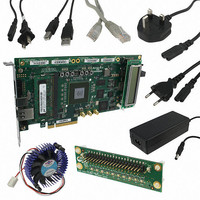
KIT DEV FPGA 2AGX260 W/6.375G TX
Manufacturer
Altera
Series
Arria II GXr
Type
FPGAr
Specifications of DK-DEV-2AGX260N
Contents
Board, Cables, CD, DVD, Power Supply
Silicon Manufacturer
Altera
Core Architecture
FPGA
Core Sub-architecture
Arria
Silicon Core Number
EP2
Silicon Family Name
Arria II GX
Rohs Compliant
Yes
For Use With/related Products
EP2AGX260
Lead Free Status / RoHS Status
Lead free / RoHS Compliant
Other names
544-2696
Available stocks
Company
Part Number
Manufacturer
Quantity
Price
Company:

Part Number:
DK-DEV-2AGX260N
Manufacturer:
Altera
Quantity:
135


Chapter 2: Board Components
Memory
Table 2–44. SSRAM Component Reference and Manufacturing Information
Flash
Table 2–45. Flash Pin Assignments, Schematic Signal Names, and Functions (Part 1 of 2)
© July 2010 Altera Corporation
Board Reference
Board Reference
U23.A1
U23.B1
U23.C1
U23.D1
U23.D2
U23.A2
U23.C2
U23.A3
U23.B3
U23.C3
U23.D3
U23.C4
U23.A5
U23.B5
U23.C5
U23.D7
U23.D8
U22
Standard Synchronous Pipelined
SCD, 512K × 36, 200 MHz
Address bus
Address bus
Address bus
Address bus
Address bus
Address bus
Address bus
Address bus
Address bus
Address bus
Address bus
Address bus
Address bus
Address bus
Address bus
Address bus
Address bus
Table 2–44
The flash interface consists of a single synchronous flash memory device, providing
64 Mbyte with a 16-bit data bus. This device is part of the shared FSM bus which
connects to the flash memory, SRAM, and MAX II CPLD EPM2210 System Controller.
There are two 512-Mbyte die per package. The parameter blocks are 32 K and main
blocks are 128 K. The parameters of this device are located at the top of the address
space.
This 16-bit data memory interface can sustain burst read operations at up to 52 MHz
for a throughput of 832 Mbps. The write performance is 270 µs for a single word and
310 µs for a 32-word buffer. The erase time is 800 ms for a 128 K main block.
Table 2–45
names and types are relative to the Arria II GX device in terms of I/O setting and
direction.
Description
Description
lists the SSRAM component reference and manufacturing information.
lists the flash pin assignments, signal names, and functions. The signal
FSM_A1
FSM_A2
FSM_A3
FSM_A4
FSM_A5
FSM_A6
FSM_A7
FSM_A8
FSM_A9
FSM_A10
FSM_A11
FSM_A12
FSM_A13
FSM_A14
FSM_A15
FSM_A16
FSM_A17
Schematic Signal Name
ISSI Inc.
Manufacturer
Arria II GX FPGA Development Board, 6G Edition Reference Manual
IS61VPS51236A-200B3
Manufacturing
Part Number
I/O Standard
2.5-V
Arria II GX Device
Manufacturer
www.issi.com
Pin Number
Website
D29
D20
A23
B24
C24
H19
K21
J21
L13
E25
F21
J19
L21
F25
C8
N9
J3
2–47
Related parts for DK-DEV-2AGX260N
Image
Part Number
Description
Manufacturer
Datasheet
Request
R

Part Number:
Description:
KIT DEV ARRIA II GX FPGA 2AGX125
Manufacturer:
Altera
Datasheet:

Part Number:
Description:
KIT DEV CYCLONE III LS EP3CLS200
Manufacturer:
Altera
Datasheet:

Part Number:
Description:
KIT DEV STRATIX IV FPGA 4SE530
Manufacturer:
Altera
Datasheet:

Part Number:
Description:
KIT DEV MAX V 5M570Z
Manufacturer:
Altera
Datasheet:

Part Number:
Description:
KIT DEV STRATIX V FPGA 5SGXEA7
Manufacturer:
Altera
Datasheet:

Part Number:
Description:
KIT DEVELOPMENT STRATIX III
Manufacturer:
Altera
Datasheet:

Part Number:
Description:
KIT DEVELOPMENT STRATIX IV
Manufacturer:
Altera
Datasheet:

Part Number:
Description:
KIT DEV ARRIA GX 1AGX60N
Manufacturer:
Altera
Datasheet:
Part Number:
Description:
KIT STARTER CYCLONE IV GX
Manufacturer:
Altera
Datasheet:
Part Number:
Description:
KIT DEVELOPMENT STRATIX IV
Manufacturer:
Altera
Datasheet:

Part Number:
Description:
CPLD, EP610 Family, ECMOS Process, 300 Gates, 16 Macro Cells, 16 Reg., 16 User I/Os, 5V Supply, 35 Speed Grade, 24DIP
Manufacturer:
Altera Corporation
Datasheet:
Part Number:
Description:
CPLD, EP610 Family, ECMOS Process, 300 Gates, 16 Macro Cells, 16 Reg., 16 User I/Os, 5V Supply, 15 Speed Grade, 24DIP
Manufacturer:
Altera Corporation
Datasheet: