DK-DEV-2AGX260N Altera, DK-DEV-2AGX260N Datasheet - Page 51
DK-DEV-2AGX260N
Manufacturer Part Number
DK-DEV-2AGX260N
Description
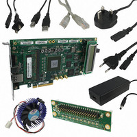
KIT DEV FPGA 2AGX260 W/6.375G TX
Manufacturer
Altera
Series
Arria II GXr
Type
FPGAr
Specifications of DK-DEV-2AGX260N
Contents
Board, Cables, CD, DVD, Power Supply
Silicon Manufacturer
Altera
Core Architecture
FPGA
Core Sub-architecture
Arria
Silicon Core Number
EP2
Silicon Family Name
Arria II GX
Rohs Compliant
Yes
For Use With/related Products
EP2AGX260
Lead Free Status / RoHS Status
Lead free / RoHS Compliant
Other names
544-2696
Available stocks
Company
Part Number
Manufacturer
Quantity
Price
Company:

Part Number:
DK-DEV-2AGX260N
Manufacturer:
Altera
Quantity:
135


Chapter 2: Board Components
Memory
Table 2–41. DDR2 SODIMM Pin Assignments, Signal Names and Functions (Part 3 of 4)
© July 2010 Altera Corporation
Board Reference
J7.123
J7.125
J7.135
J7.137
J7.124
J7.126
J7.134
J7.136
J7.130
J7.131
J7.129
J7.141
J7.143
J7.151
J7.153
J7.140
J7.142
J7.152
J7.154
J7.147
J7.148
J7.146
J7.157
J7.159
J7.173
J7.175
J7.158
J7.160
J7.174
J7.176
J7.170
J7.169
J7.64
J7.74
J7.76
J7.67
J7.70
J7.68
Data bus byte lane 3
Data bus byte lane 3
Data bus byte lane 3
Write mask byte lane 3
Data strobe P byte lane 3
Data strobe N byte lane 3
Data bus byte lane 4
Data bus byte lane 4
Data bus byte lane 4
Data bus byte lane 4
Data bus byte lane 4
Data bus byte lane 4
Data bus byte lane 4
Data bus byte lane 4
Write mask byte lane 4
Data strobe P byte lane 4
Data strobe N byte lane 4
Data bus byte lane 5
Data bus byte lane 5
Data bus byte lane 5
Data bus byte lane 5
Data bus byte lane 5
Data bus byte lane 5
Data bus byte lane 5
Data bus byte lane 5
Write mask byte lane 5
Data strobe P byte lane 5
Data strobe N byte lane 5
Data bus byte lane 6
Data bus byte lane 6
Data bus byte lane 6
Data bus byte lane 6
Data bus byte lane 6
Data bus byte lane 6
Data bus byte lane 6
Data bus byte lane 6
Write mask byte lane 6
Data strobe P byte lane 6
Description
DDR2_DQ29
DDR2_DQ30
DDR2_DQ31
DDR2_DM3
DDR2_DQS3
DDR2_DQSN3
DDR2_DQ32
DDR2_DQ33
DDR2_DQ34
DDR2_DQ35
DDR2_DQ36
DDR2_DQ37
DDR2_DQ38
DDR2_DQ39
DDR2_DM4
DDR2_DQS4
DDR2_DQSN4
DDR2_DQ40
DDR2_DQ41
DDR2_DQ42
DDR2_DQ43
DDR2_DQ44
DDR2_DQ45
DDR2_DQ46
DDR2_DQ47
DDR2_DM5
DDR2_DQS5
DDR2_DQSN5
DDR2_DQ48
DDR2_DQ49
DDR2_DQ50
DDR2_DQ51
DDR2_DQ52
DDR2_DQ53
DDR2_DQ54
DDR2_DQ55
DDR2_DM6
DDR2_DQS6
Schematic Signal
Name
Arria II GX FPGA Development Board, 6G Edition Reference Manual
1.8-V SSTL Class I
I/O Standard
Pin Number
Arria II GX
Device
AM18
AM16
AM17
AN19
AK18
AP20
AL18
AP15
AN15
AH17
AC18
AE17
AP14
AN13
AH18
AH16
AH15
AP10
AL16
AK16
AP12
AN12
AG16
AK15
AL15
AL14
AE16
AL11
AC15
AK13
AF18
AF17
AF16
AP9
AN7
AP7
AP6
AP5
2–43
Related parts for DK-DEV-2AGX260N
Image
Part Number
Description
Manufacturer
Datasheet
Request
R

Part Number:
Description:
KIT DEV ARRIA II GX FPGA 2AGX125
Manufacturer:
Altera
Datasheet:

Part Number:
Description:
KIT DEV CYCLONE III LS EP3CLS200
Manufacturer:
Altera
Datasheet:

Part Number:
Description:
KIT DEV STRATIX IV FPGA 4SE530
Manufacturer:
Altera
Datasheet:

Part Number:
Description:
KIT DEV MAX V 5M570Z
Manufacturer:
Altera
Datasheet:

Part Number:
Description:
KIT DEV STRATIX V FPGA 5SGXEA7
Manufacturer:
Altera
Datasheet:

Part Number:
Description:
KIT DEVELOPMENT STRATIX III
Manufacturer:
Altera
Datasheet:

Part Number:
Description:
KIT DEVELOPMENT STRATIX IV
Manufacturer:
Altera
Datasheet:

Part Number:
Description:
KIT DEV ARRIA GX 1AGX60N
Manufacturer:
Altera
Datasheet:
Part Number:
Description:
KIT STARTER CYCLONE IV GX
Manufacturer:
Altera
Datasheet:
Part Number:
Description:
KIT DEVELOPMENT STRATIX IV
Manufacturer:
Altera
Datasheet:

Part Number:
Description:
CPLD, EP610 Family, ECMOS Process, 300 Gates, 16 Macro Cells, 16 Reg., 16 User I/Os, 5V Supply, 35 Speed Grade, 24DIP
Manufacturer:
Altera Corporation
Datasheet:
Part Number:
Description:
CPLD, EP610 Family, ECMOS Process, 300 Gates, 16 Macro Cells, 16 Reg., 16 User I/Os, 5V Supply, 15 Speed Grade, 24DIP
Manufacturer:
Altera Corporation
Datasheet: